MAX12527
Detailed Description
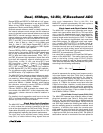
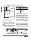
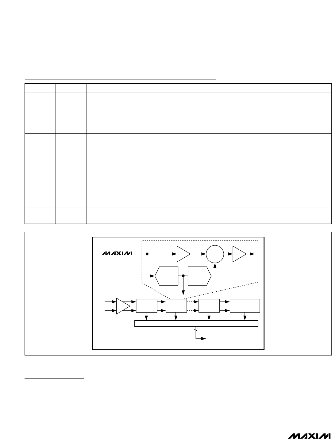
The MAX12527 uses a 10-stage, fully differential,
pipelined architecture (Figure 1) that allows for high-
speed conversion while minimizing power consump-
tion. Samples taken at the inputs move progressively
through the pipeline stages every half clock cycle.
From input to output the total latency is 8 clock cycles.
Each pipeline converter stage converts its input voltage
to a digital output code. At every stage, except the last,
the error between the input voltage and the digital out-
put code is multiplied and passed along to the next
pipeline stage. Digital error correction compensates for
ADC comparator offsets in each pipeline stage and
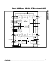
ensures no missing codes. Figure 2 shows the
MAX12527 functional diagram.
Dual, 65Msps, 12-Bit, IF/Baseband ADC
14 ______________________________________________________________________________________
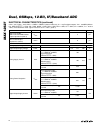
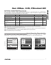
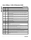
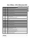
PIN NAME FUNCTION
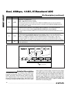
66 SHREF
Shared Reference Digital Input.
SHREF = V
DD
: Shared reference enabled.
SHREF = GND: Shared reference disabled.
When sharing the reference, externally connect REFAP and REFBP together to ensure that V
REFAP
equals V
REFBP
. Similarly, when sharing the reference, externally connect REFAN to REFBN together to
ensure that V
REFAN
= V
REFBN
.
67
REFOUT
Internal Reference Voltage Output. The REFOUT output voltage is 2.048V and REFOUT can deliver 1mA.
For internal reference operation, connect REFOUT directly to REFIN or use a resistive divider from
REFOUT to set the voltage at REFIN. Bypass REFOUT to GND with a ≥0.1µF capacitor.
For external reference operation, REFOUT is not required and must be bypassed to GND with a ≥0.1µF
capacitor.
68 REFIN
Single-Ended Reference Analog Input.
For internal reference and buffered external reference operation, apply a 0.7V to 2.3V DC reference
voltage to REFIN. Bypass REFIN to GND with a 4.7µF capacitor. Within its specified operating voltage,
REFIN has a >50MΩ input impedance, and the differential reference voltage (V
REF_P
- V
REF_N
) is
generated from REFIN. For unbuffered external reference operation, connect REFIN to GND. In this
mode REF_P, REF_N, and COM_ are high-impedance inputs that accept the external reference voltages.
—EP
Exposed Paddle. EP is internally connected to GND. Externally connect EP to GND to achieve specified
dynamic performance.
Pin Description (continued)
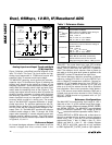
MAX12527
Σ
+
−
DIGITAL ERROR CORRECTION
FLASH
ADC
x2
DAC
STAGE 2
IN_P
IN_N
STAGE 1 STAGE 9
STAGE 10
END OF PIPELINE
D0_ THROUGH D11_
Figure 1. Pipeline Architecture—Stage Blocks


