


KE-32TS2U(UC) 3-6
Note:
• All capacitors are in µF unless otherwise noted. (pF: µµF)
Capacitors without voltage indication are all 50 V.
• Indication of resistance, which does not have one for rating electrical
power, is as follows.
Pitch: 5 mm
Rating electrical power 1/4 W (CHIP : 1/10 W)
• All resistors are in ohms.
• : nonflammable resistor.
• : fusible resistor.
•
T : internal component.
• : panel designation, and adjustment for repair.
• All variable and adjustable resistors have characteristic curve B, unless
otherwise noted.
• : earth-ground.
• : earth-chassis.
• When replacing the part in below table, be sure to perform the related
adjustment.
• All voltages are in V.
• Readings are taken with a 10 M digital multimeter.
• Readings are taken with a color-bar signal input.
• Voltage variations may be noted due to normal production tolerances.
•
*
: Can not be measured.
• Circled numbers are waveform references.
• : B + bus.
• :B – bus.
Note: The components identified by shading and
mark ! are critical for safety. Replace only
with part number specified.
Note: Les composants identifiés par un tramé et
une marque ! sont critiques pour la
sécurité. Ne les remplacer que par une pièce
portant le numéro spécifié.
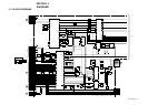
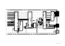
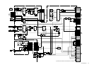
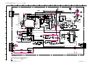
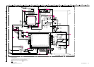
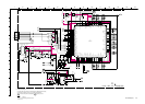
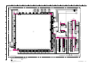
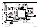
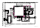
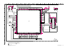
3-3. SCHEMATIC DIAGRAMS AND PRINTED WIRING BOARDS
• Divided circuit diagram
One sheet of B and Q boards are circuit diagram is divided into three sheets,
each having the code B-a to B-c. For example, the destination
ab1 on the code B-a sheet is connected to ab1 on the B-b sheet.
a b 1
Ref. No.
Circuit diagram division code
G
D
S
B1 E1
C2
B2 C1
E2
2
3
4
5
6
7
8
9
0
!¡
!™
!¢
!§
!¶
!•
–
1
G
D
S
B2 E2
C1
B1 C2
E1
B2 E2
C1
B1 C2
E1
B2 E2
C1
B1 C2
E1
!ª
B1 E1
E2
C1(B2)
C2
@º
B1
E2
C1
C2
@™
@£
(B2)
E1
(B2)
E1
E2
B1
C2
C1
@¡
B1
E1
C2
B2
C1
E2
G
S
S
D
G
D
B1
E1
C2
B2
C1
E2
B1
E2
C2C1(B2)
E2
B1
C1
C2E1(B2)
C2
B1
C1
E2E1(B2)
C2
B1
C1
E2
B2
E1
C2
Ver.1.6
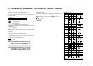
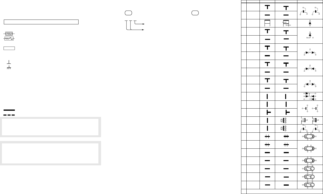
Transistor
(FET)
Transistor
Transistor
Transistor
Transistor
Transistor
Transistor
Transistor
Transistor
Transistor
Discrete semiconductot
(Chip semiconductors that are not actually used are included.)
Diode
Diode
Diode
Diode
Diode
Diode
Diode
Diode
Diode
Diode
Source
Source
Anode
Anode
(NC)
(NC)
Cathode
Anode
Cathode
Common
Cathode
Cathode
Common
Cathode
Cathode
Common
Common
Common
Common
Cathode
Anode
Base
Emitter
Collector
Base
Emitter
Collector
Drain
Gate
Gate
Drain
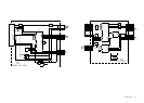
Device Printed symbol Terminal name
Circuit
Terminal name of semiconductors in silk screen
printed circuit ( )
Anode
Anode
Anode Cathode
Anode Anode
Cathode
!£
Transistor
(FET)
Transistor
(FET)
!∞
Emitter
Collector
Base
Transistor
Source
Gate
Drain
Cathode
Anode
Anode
Cathode
Anode
Anode
*