29
TDA 1519B(AUDIO OUTPUT AMPLIFIER); 2 SPEAKER MODEL
(1) Features
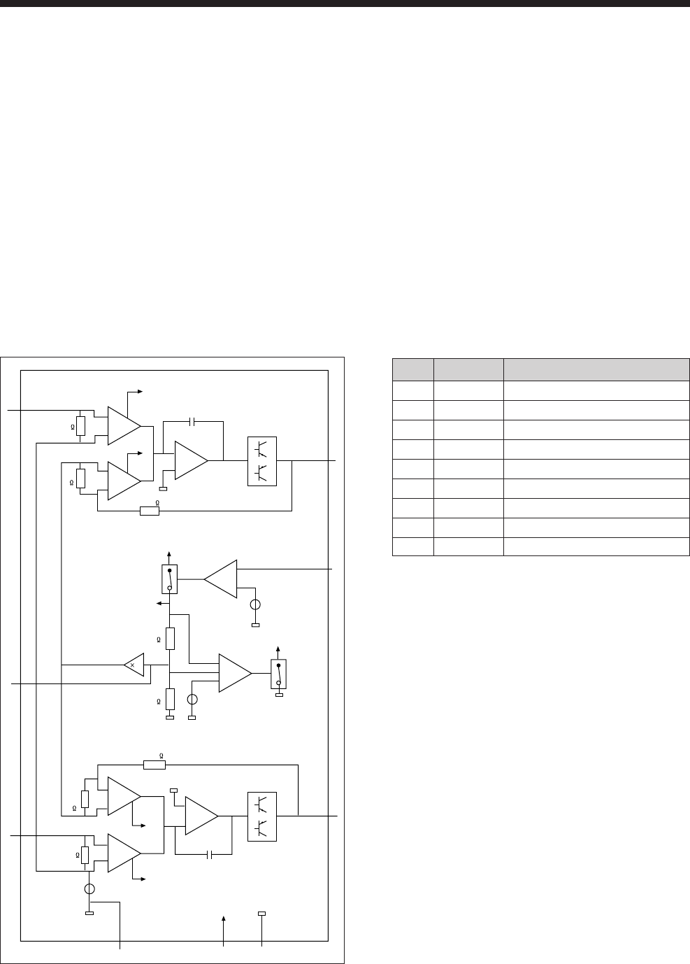
(2) General Description
The TDA 1519B is an integrated class-B dual output amplifier in a 9-lead single in-line(SIL) plastic
medium power package. The device is primarily developed for car radio applications.
(3) Block Diagram
Mute Switch
Power Stage
Vp
Vp
Stand-by
Switch
Mute
Switch
Mute Switch
TDA1519B
Stand-by
Reference
Voltage
Input
Reference
Voltage
Signal
Ground
Power
Ground
(Substrate)
Mute
Reference
Voltage
Cm
VA
VA
VA
+
1
-
+
+
-
60k
18.1k
15k
183
60k
15k
18.1k
133
4
8
6
3
9
1
Cm
Power Stage
•
Requires very few external components for
Bridge Tied Load(BTL)
• Stereo ot BTL application
• High output power
• Low offset voltage at output (important for BTL)
• Fixed gain
• Good ripple rejection
• Mute/stand-by switch
• Load dump protection
• AC and DC short-circuit-safe to ground and Vp
• Thermally protected
• Reverse polarity safe
• Capability to handle high energy on
outputs(Vp=OV)
• No switch-on/switch-off plop
• Protected against electrostatic discharge
• Identical inputs(inverting and non-inverting)
• Compatible with TDA 1519A(except output power)
(4) Pin Description
1 NINV non-inverting input
2 GND1 ground(signal)
3 RR supply voltage ripple rejection
4 OUT1 output 1
5 GND2 ground(substrate)
6 OUT2 output 2
7 Vp positive supply voltage
8 M/ss mute/stand-by switch
9 INV inverting input
PIN SYMBOL DESCRIPTION


