


CP-520/520A/520F Service Manual
DTV R&D Europe
28
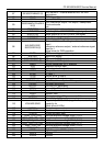
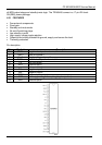
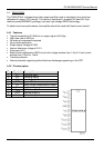
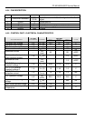
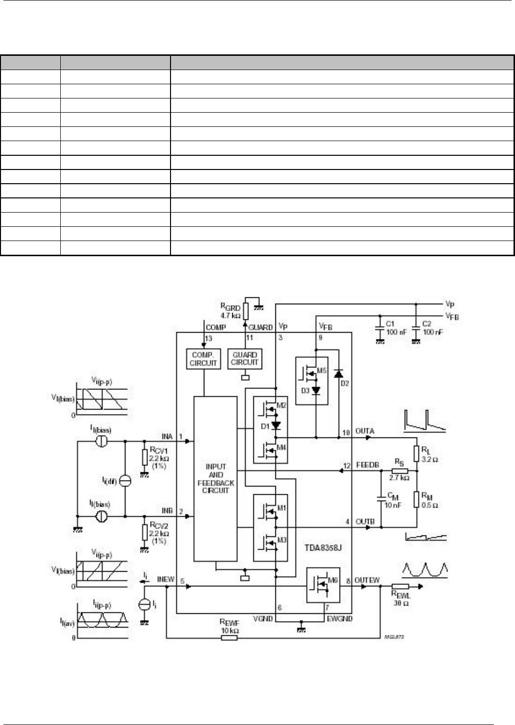
Pinning
Pin Symbol Description
1 INA Positeve vertical input
2 INB Negative vertical input
3 V
P
Supply voltage
4 OUTB Vertical output voltage B
5 INEW East-west input voltage
6 VGND Vertical ground
7 EWGND East-west ground
8 OUTEW East-west output voltage
9 V
FB
Flyback supply voltage
10 OUTA Vertical output voltage A
11 GUARD Guard output voltage
12 FEEDB Input measuring resistor
13 COMP Input compensation current
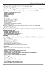
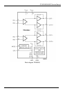
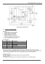
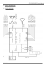
Block diagram TDA8358J