CP-520/520A/520F Service Manual
DTV R&D Europe
30
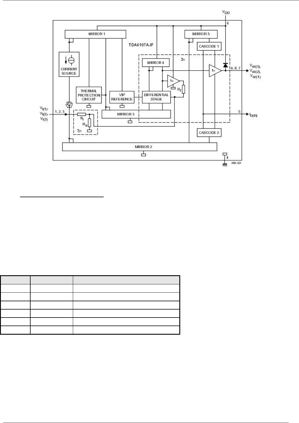
Block diagram TDA6107AJF
4.5 24WC16 - 16 KB EEPROM
Features :
§ 16 Kbit serial I2C bus EEPROM
§ 400KHz I2C Bus Compatible
§ supply voltage : 1.8 V to 6.0 V
§ Low Power CMOS Technology
§ 1 Million Erase/Write cycles (minimum)
§ 100 year data retention (minimum)
Pin description
Pin No. Name Description
1, 2, 3 A0, A1, A2 Device address – not used
5 SDA Serial Data/Address Input/Output
6 SCL Serial clock
7 WP Write control
8 Vcc Supply voltage
4 Vss Ground
The memory device is compatible with the I2C memory standard. This is a two wire serial
interface that uses a bi-directional data bus and serial clock. The memory carries a built-in 4-bit
unique device type identifier code (1010) in accordance with the I2C bus definition.
Serial Clock (SCL)
The SCL input is used to strobe all data in and out of the memory.
Serial Data (SDA)
The SDA pin is bi-directional, and is used to transfer data in or out of the memory.


