ADC12V170 Evaluation Board User’s Guide
N - 5 - www.national.com
Rev 0.0
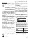
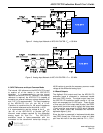
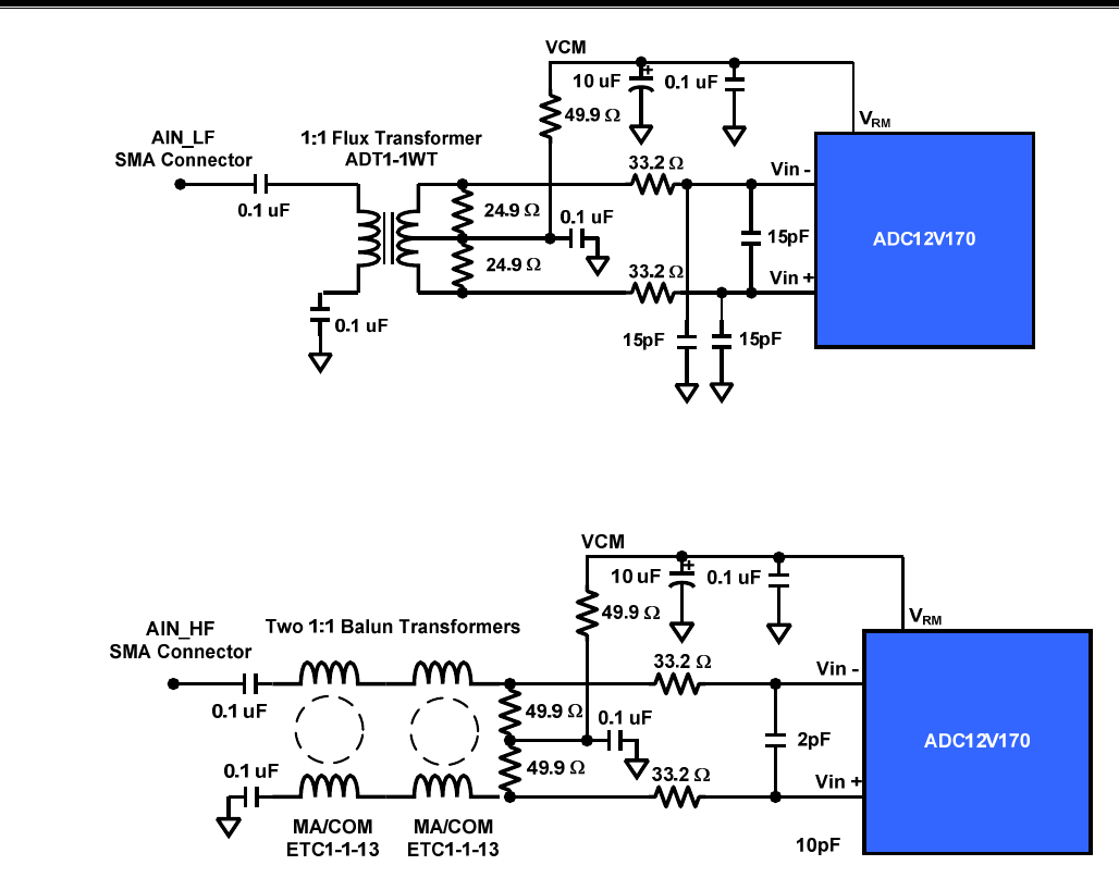
Figure 2. Analog Input Network of ADC12V170LFEB: F
IN
< 150 MHz
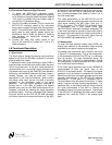
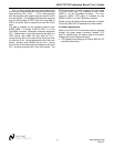
Figure 3. Analog Input Network of ADC12V170HFEB: F
IN
> 150 MHz
4.3 ADC Reference and Input Common Mode
The internal 1.0V reference on the ADC12V170 is used
to acquire all of the results in the ADC12V170
datasheet. It is recommended to use the internal
reference on the ADC12V170. However, if an external
reference is required, the ADC12V170 is capable of
accepting an external reference voltage between 0.9V
and 1.1V (1.0V recommended). The input impedance
of the ADC12V170 V
REF
pin (pin 46) is 9 kΩ.
Therefore, to overdrive this pin, the output impedance
of the exernal reference source should be << 9 kΩ.
It is recommended to use the voltage at the V
RM
pin
(pin 45) of the ADC12V170 to provide the 1.5V
common mode voltage required for the differential
analog inputs V
IN+
and V
IN-
. The ADC12V170
evaluation board is factory-assembled with V
RM
connected to the transformer center-tap through a
49.9Ω resistor to provide the necessary common mode
voltage to the differential analog input.
4.4 Board Outputs
The digitized 12-bit output word from the ADC12V170
evaluation board is presented in interleaved double
data rate (DDR) format. The digital output lines from
the ADC12V170 evaluation board consist of 16 lines
which are arranged into 8 LVDS pairs. These 8 pairs
of lines carry the 12-bit output data (6 pairs), the DRDY
signal which should be used to capture the output data
(1 pair) and the over-range bit (OVR) which indicates
that the digital output has exceeded the maximum
digitizable signal (1 pair).
Since the data is presented in interleaved double data
rate (DDR) format, the 12-bit word is output on 6 data
pair lines with half of the data (odd bits: D1+/-, D3+/-,


