


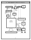
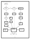
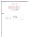
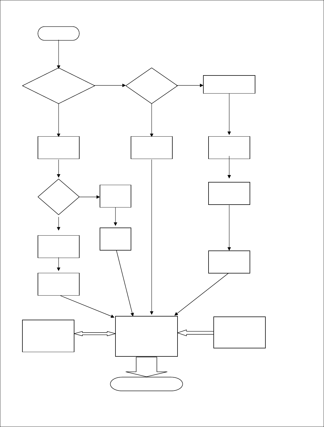
Video Signal Processing Block Diagram
29
Power on
Input signal set to
Tuner or
Composite?
N
Y
Input signal
set to HDMI?
N
Input signal set to
Component or VGA
Process
Circuit
Y
Y
Process
Circuit
Process
Circuit
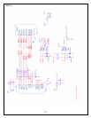
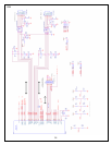
MST9883
ADC
ATSC
digital
signal
Y
Oren
CAS-220
N
FMS6408
ZR39660
(Main Chip)
DDR333 RAM
512M
(256M*2)
SDRAM 32M
LVDS
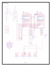
Switch Chip
FSAV330/331
Switch Chip
FSAV330/331
X6941
IF Filter