


– 3 –
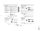
KV-HF21M80
RM-952
TABLE OF CONTENTS
Section Title Page
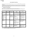
SELF DIAGNOSIS FUNCTION................................ 4
1. GENERAL ........................................................................ 8
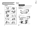
2. DISASSEMBLY
2-1. Rear Cover Removal ................................................ 19
2-2. Chassis Assy Removal ............................................. 19
2-3. F Bracket Removal .................................................. 19
2-4. Service Position ....................................................... 19
2-5. Replacement of Parts ............................................... 20
2-5-1. Replacement of Control Button ....................... 20
2-5-2. Replacement of Light Guide ............................ 20
2-6. Terminal Bracket Removal ...................................... 20
2-7. Degauss Coil Removal............................................. 20
2-8. Picture Tube Removal.............................................. 21
3. SET-UP ADJUSTMENTS
3-1. Beam Landing .......................................................... 22
3-2. Convergence............................................................. 23
3-3. Focus Adjustment .................................................... 25
3-4. G2 (Screen) and White Balance Adjustments......... 25
4. CIRCUIT ADJUSTMENT
4-1. Adjustments with Commander ................................ 26
4-2. Adjustment Method ................................................. 27
4-3. Picture Quality Adjustments.................................... 32
4-4. A Board Adjustment After IC003 (Memory)
Replacement............................................................. 32
4-5. Picture Distortion Adjustment ................................. 33
Section Title Page
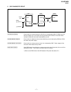
5. DIAGRAMS
5-1. Block Diagram ......................................................... 37
5-2. Frame Schematic Diagram ...................................... 40
5-3 Circuit Boards Location .......................................... 42
5-4. Schematic Diagrams and Printed Wiring Boards ... 43
(1) Schematic Diagram of A (1/2) Board...................... 45
(2) Schematic Diagram of A (2/2) Board...................... 48
(3) Schematic Diagram of C3 Board ............................ 54
(4) Schematic Diagram of F Board ............................... 57
5-5. Semiconductors........................................................ 59
6. EXPLODED VIEW
6-1. Chassis ..................................................................... 61
7. ELECTRICAL PARTS LIST....................................... 63