


www.ti.com
2Introduction
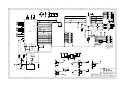
3AnalogInterface
3.1AnalogInput–ChannelA0
Introduction
TheADS8364andADS8365arehigh-speed,low-power,6-channel,16-bitA/Dconvertersthatoperate
fromindependent+5-VAvddandDvddsupplies.Internalbuffercircuitspoweredfrom3.3-Vto5.5-VBVdd
suppliesallowformixedlogicleveloperationwithoutadditionalleveltranslation.
Thesixinputchannelscontainfullydifferentialsample-and-holdcircuitswhicharedividedintothreepairs
(A,B,andC).Eachchannelpairhasaholdsignal(HOLDA,HOLDB,andHOLDC)which,whenstrobed
together,providessimultaneoussamplingonallsixanaloginputs.Thedevicesacceptanaloginput
voltagesintherangeof–V
REF
to+V
REF
.Thepartsalsoacceptbipolarinputrangeswhenalevelshift
circuitisusedintheanalogfront-endcircuitry(seeFigure1).
ConversiontimefortheADS8364andADS8365is3.2µswhena5-MHzexternalclockisused.The
correspondingacquisitiontimeis800ns.Toachievemaximumoutputrate(250kHzperchannel,effective
1.5-MSPSthroughputmax),thereadfunctioncanbeperformedduringthestartofthenextconversion.
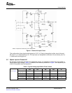
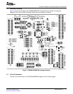
TheanaloginputtotheEVMisdividedintwoparts.ConnectorJ4providesaccesstoinputchannelsA0
andA1throughtwodifferentamplifiercircuitconfigurations.TheinputbufferconfigurationofchannelA0
presentsatypicalfront-endcircuitfortheA/Dconverter.Itsfunctionistoprovidelevelandimpedance
adaptationoftheinputsignal.TheinputtochannelA1isabipolarconfigurationusingtheINA159to
accommodate±10-Vinputsignals.ConnectorJ3providesaccesstotheremaininganaloginputchannels
throughsimpleR/Cfilters.
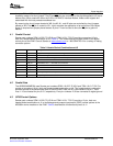
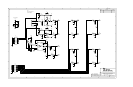
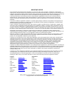
TheanaloginputtotheADS8364/65MEVMboardforchannelA0iscomposedofthedualOPA2132
operationalamplifieranditsassociatedcircuitryasshowninFigure1.TheOPA2132ispoweredfromthe
±12-Vanalogsupply,andarrangedasaninvertingamplifierwithagainof1.Theinternal+2.5-V
referencevoltageoftheADS8364orADS8365isappliedtothenoninvertinginputoftheOPA2132to
provideinputbias.
2ADS8364/65MEVMSLAU189–September2006
SubmitDocumentationFeedback