CY62147DV18
MoBL2™
Document #: 38-05343 Rev. *B Page 5 of 11
wqewqewq
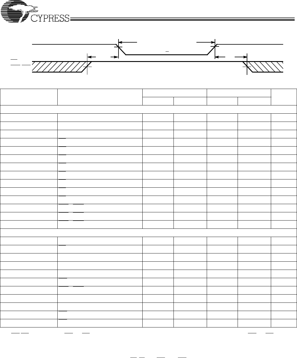
Data Retention Waveform
[9]
Switching Characteristics Over the Operating Range
[10.]
Parameter Description
55 ns 70 ns
UnitMin. Max. Min. Max.
Read Cycle
t
RC
Read Cycle Time 55 70 ns
t
AA
Address to Data Valid 55 70 ns
t
OHA
Data Hold from Address Change 10 10 ns
t
ACE
CE LOW to Data Valid 55 70 ns
t
DOE
OE LOW to Data Valid 25 35 ns
t
LZOE
OE LOW to LOW Z
[11]
5 5 ns
t
HZOE
OE HIGH to High Z
[11, 12]
16 16 ns
t
LZCE
CE LOW to Low Z
[11]
10 10 ns
t
HZCE
CE HIGH to High Z
[11, 12]
20 25 ns
t
PU
CE LOW to Power-Up 0 0 ns
t
PD
CE HIGH to Power-Down 55 70 ns
t
DBE
BLE / BHE LOW to Data Valid 55 70 ns
t
LZBE
BLE / BHE LOW to Low Z
[11]
10 10 ns
t
HZBE
BLE / BHE HIGH to HIGH Z
[11, 12]
20 25 ns
Write Cycle
[13]
t
WC
Write Cycle Time 55 70 ns
t
SCE
CE LOW to Write End 40 50 ns
t
AW
Address Set-up to Write End 40 50 ns
t
HA
Address Hold from Write End 0 0 ns
t
SA
Address Set-up to Write Start 0 0 ns
t
PWE
WE Pulse Width 40 45 ns
t
BW
BLE / BHE LOW to Write End 40 50 ns
t
SD
Data Set-Up to Write End 25 30 ns
t
HD
Data Hold from Write End 0 0 ns
t
HZWE
WE LOW to High-Z
[11, 12]
20 25 ns
t
LZWE
WE HIGH to Low-Z
[11]
10 10 ns
Notes:
9. BHE.BLE is the AND of both BHE and BLE. Chip can be deselected by either disabling the chip enable signal or by disabling both BHE and BLE.
10. Test conditions for all parameters other than three-state parameters assume signal transition time of 1V/ns or less, timing reference levels of V
CC(typ)
/2, input
pulse levels of 0 to V
CC(typ.)
, and output loading of the specified I
OL
/I
OH
as shown in the “AC Test Loads and Waveforms” section.
11. At any given temperature and voltage condition, t
HZCE
is less than t
LZCE
, t
HZBE
is less than t
LZBE
, t
HZOE
is less than t
LZOE
, and t
HZWE
is less than t
LZWE
for any
given device.
12. t
HZOE
, t
HZCE
, t
HZBE
, and t
HZWE
transitions are measured when the outputs enter a high impedence state.
13. The internal Write time of the memory is defined by the overlap of WE, CE
= V
IL
, BHE and/or BLE = V
IL
. All signals must be ACTIVE to initiate a write and any
of these signals can terminate a write by going INACTIVE. The data input set-up and hold timing should be referenced to the edge of the signal that terminates
the write.
V
CC(min)
V
CC(min)
t
CDR
V
DR
> 1.0 V
DATA RETENTION MODE
t
R
V
CC
CE or
BHE
.BLE
[+] Feedback


