1999 May 10 7
Philips Semiconductors Preliminary specification
Universal Serial Bus (USB) CODEC UDA1325
V
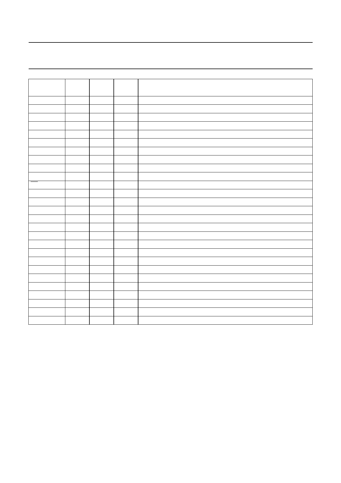
DDA1
38 29 − analog supply voltage 1
V
SSA1
39 30 − analog ground 1
V
ref(DA)
40 31 O reference voltage output DAC
V
ref(AD)
41 32 O reference voltage output ADC
V
DDA2
42 33 − analog supply voltage 2
VINL 43 34 I input signal left channel PGA
V
SSA2
44 35 − analog ground 2
n.c. 45 −−not connected
n.c. 46 −−not connected
VINR 47 36 I input signal right channel PGA
EA 48 −−external access (active LOW)
VRN 49 37 I negative reference input voltage ADC
ALE 50 −−address latch enable (active HIGH)
VRP 51 38 I positive reference input voltage ADC
V
DDA3
52 39 − supply voltage for crystal oscillator and analog PLL
XTAL2a 53 40 O crystal output (analog; ADC)
XTAL1a 54 41 I crystal input (analog; ADC)
V
SSA3
55 42 − crystal oscillator and analog PLL ground
P0.0 56 − I/O Port 0.0 of the microcontroller
DA 57 1 I data Input (digital)
P0.1 58 − I/O Port 0.1 of the microcontroller
WS 59 2 I word select Input (digital)
P0.2 60 − I/O Port 0.2 of the microcontroller
BCK 61 3 I bit clock Input (digital)
P0.3 62 − I/O Port 0.3 of the microcontroller
GP2/DO 63 4 I/O general purpose pin 2 or data output
P0.4 64 − I/O Port 0.4 of the microcontroller
SYMBOL
PIN
QFP64
PIN
SDIP42
I/O DESCRIPTION


