


MAX12557
select either one-half or one-fourth of the clock speed for
sampling provides design flexibility, relaxes clock
requirements, and can minimize clock jitter.
System Timing Requirements
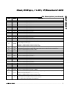
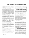
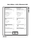
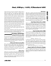
Figure 5 shows the timing relationship between the
clock, analog inputs, DAV indicator, DOR_ indicators,
and the resulting output data. The analog input is sam-
pled on the falling (rising) edge of CLKP (CLKN) and
the resulting data appears at the digital outputs 8 clock
cycles later.
The DAV indicator is synchronized with the digital out-
put and optimized for use in latching data into digital
back-end circuitry. Alternatively, digital back-end cir-
cuitry can be latched with the rising edge of the con-
version clock (CLKP - CLKN).
Data-Valid Output
DAV is a single-ended version of the input clock that is
compensated to correct for any input clock duty-cycle
variations. The MAX12557 output data changes on the
falling edge of DAV, and DAV rises once the output
data is valid. The falling edge of DAV is synchronized
to have a 5.4ns delay from the falling edge of the input
clock. Output data at D0A/B–D13A/B and DORA/B are
valid from 7ns before the rising edge of DAV to 7ns
after the rising edge of DAV.
DAV enters high impedance when the MAX12557 is
powered down (PD = OV
DD
). DAV enters its high-
impedance state 10ns after the rising edge of PD and
becomes active again 10ns after PD transitions low.
DAV is capable of sinking and sourcing 600µA and has
three times the driving capabilities of D0A/B–D13A/B
and DORA/B. DAV is typically used to latch the
MAX12557 output data into an external digital back-end
circuit. Keep the capacitive load on DAV as low as possi-
ble (<15pF) to avoid large digital currents feeding back
into the analog portion of the MAX12557, thereby
degrading its dynamic performance. Buffering DAV
Dual, 65Msps, 14-Bit, IF/Baseband ADC
18 ______________________________________________________________________________________
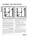
MAX12557
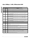
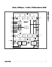
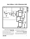
CLKP
CLKN
V
DD
GND
10kΩ
10kΩ
10kΩ
10kΩ
DUTY-CYCLE
EQUALIZER
S
1H
S
2H
S
2L
S
1L
SWITCHES S
1_
AND S
2_
ARE OPEN
DURING POWER-DOWN MAKING
CLKP AND CLKN HIGH IMPEDANCE.
SWITCHES S
2_
ARE OPEN IN
SINGLE-ENDED CLOCK MODE.
Figure 4. Siimplified Clock Input Circuit
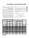
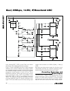
DIV4 DIV2 FUNCTION
00
Clock Divider Disabled
f
SAMPLE
= f
CLK
01
Divide-by-Two Clock Divider
f
SAMPLE
= f
CLK
/ 2
10
Divide-by-Four Clock Divider
f
SAMPLE
= f
CLK
/ 4
11Not Allowed
Table 2. Clock-Divider Control Inputs
DAV
N
N + 1
N +2
N + 3
N + 4
N + 5
N + 6
N + 7
N + 8
N + 9
t
DAV
t
SETUP
t
AD
N - 1
N - 2
N - 3
t
HOLD
t
CL
t
CH
DIFFERENTIAL ANALOG INPUT (IN_P–IN_N)
CLKN
CLKP
(V
REF_P
- V
REF_N
) x 2/3
(V
REF_N
- V
REF_P
) x 2/3
N + 4
D0_–D13_
DOR
8.0 CLOCK-CYCLE DATA LATENCY
t
SETUP
t
HOLD
NN + 1 N + 2 N + 3 N + 5 N + 6 N + 7N - 1N - 2N - 3 N + 9N + 8
Figure 5. System Timing Diagram