13
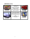
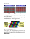
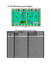
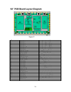
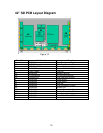
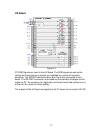
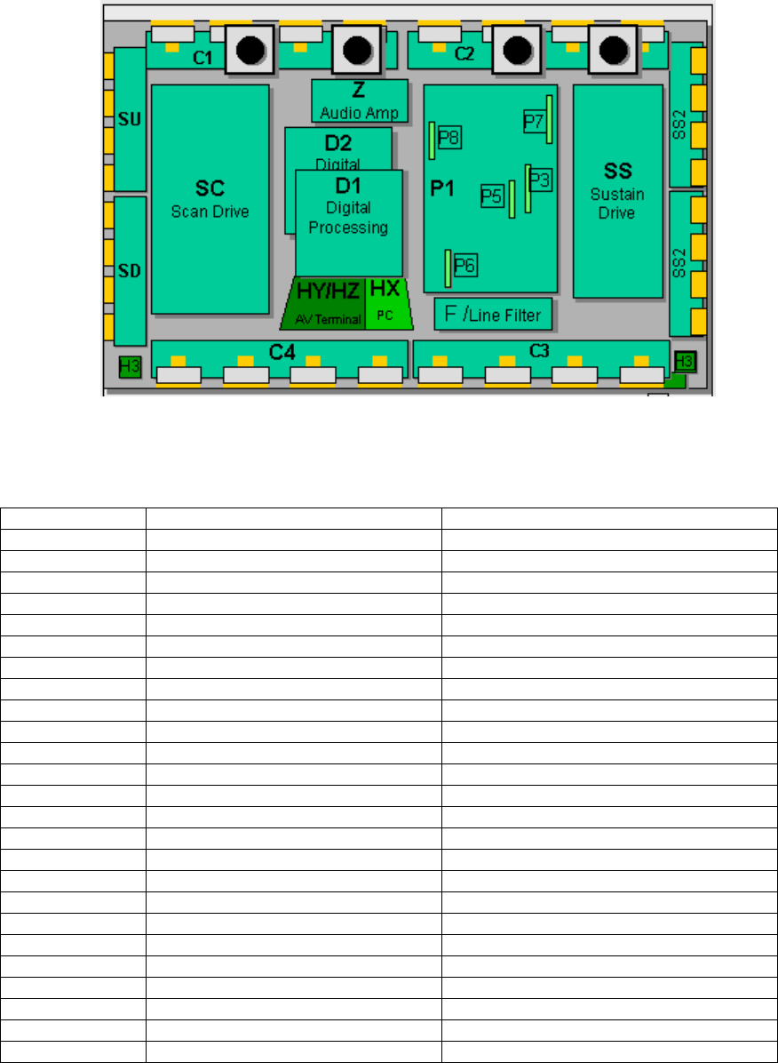
42” HD PCB Board Layout Diagram
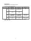
Printed Circuit Board Information Table
Board Name Part Number Function
C1 TNPA2428 Data Drive (Upper Left)
C2 TNPA2429 Data Drive (Upper Right)
C3 TNPA2430 Data Drive (Lower Right)
C4 TNPA2431 Data Drive (Lower Left)
D1 TZTNP01LLSB Format Converter
D2 TNPA2427 Plasma AI Sub-Field Processor
F TNPA2444 Line filter
H3 TNPA2249 Speaker terminal
HX TZTNP01LLSU PC type Input terminal
HZ TXNHZ40JJS RCA type Input terminal
P TXN/P10LLS Power supply
P3 TNPA2439 Drive voltage oscillator
P5 TNPA2440 Primary oscillator
P6 TNPA2441 PFC oscillator
P7 TNPA2442 Drive voltage protection
P8 TNPA2443 Process voltage protection
S1 TNPA2283AC Power switch
SC TNPA2434 Scan out
SD TNPA2433 Scan connection (Lower)
SS TNPA2435 Sustain out
SS2 TNPA2436 Sustain connection (Upper)
SS3 TNPA2437 Sustain connection (Lower)
SU TNPA2432 Scan connection (Upper)
V1 TNPA2282AC Front SW. & Remote receiver
Z TNPA2445 Audio out
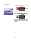
Figure 10


