


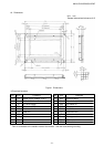
AN.No.G1216B1N000-3D0E
- 9 -
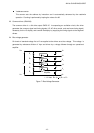
2.2.2 Functions and Operations of Main Blocks
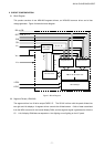
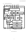
(1) Interface Control Unit
The interface control unit consists of the following blocks:
Input and output buffer
Input and output register
Instruction register
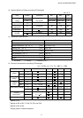
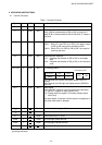
The above blocks are selected according to the following combinations of R/W and D/I signals:
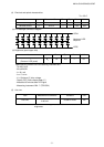
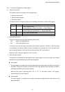
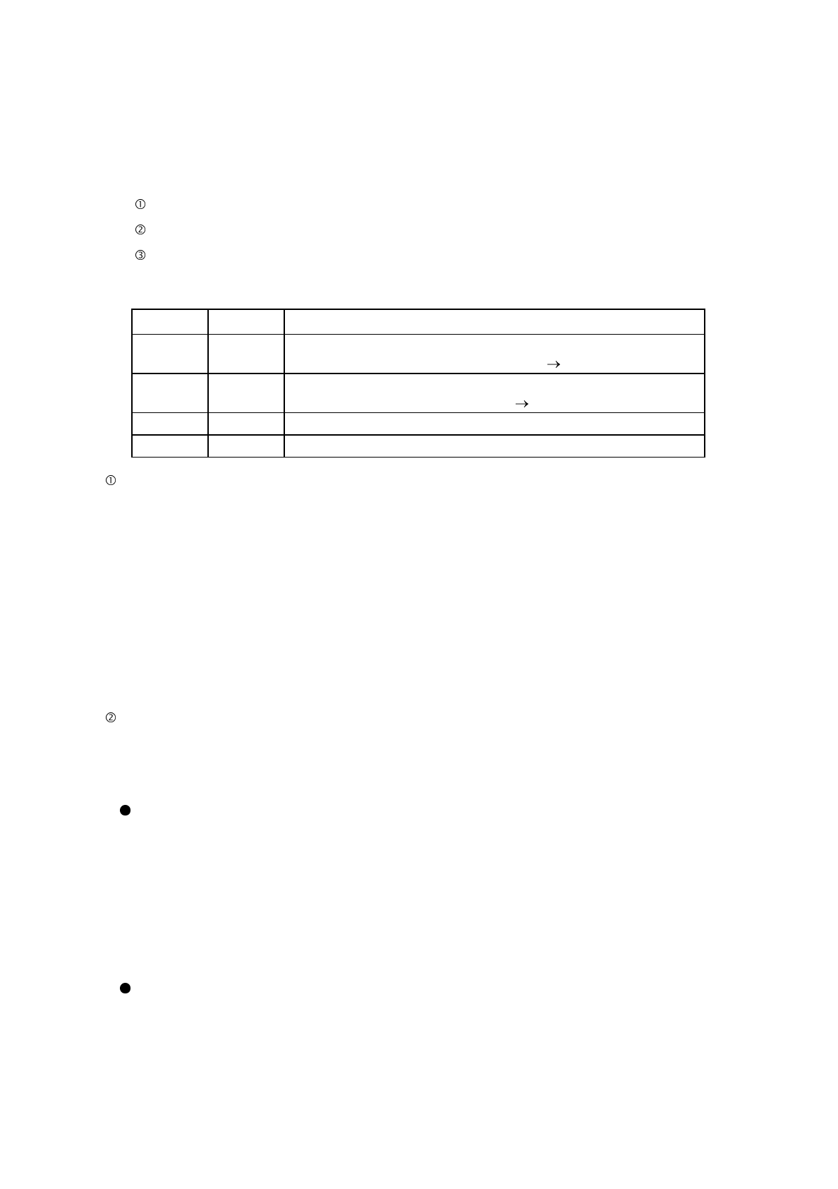
D / I R / W Functions
1 1 Output Register Read
Internal Operation (Display Data RAM Output Register)
10
Input Register Write
Internal Operation (Input Resister Display Data RAM)
0 1 Busy Check and Status Read
0 0 Instruction
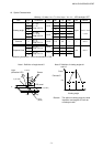
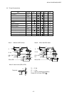
Input and output buffer
The data is transmitted through eight data buses (DB
0
to DB
7
).
DB
7
....... MSB (most significant bit)
DB
0
...... LSB (least significant bit)
The data can be input and output only when the Chip Select is selected. Therefore, if the Chip Select
is not selected, the internal condition remains unchanged and instruction will not be executed, even
when changing the signal of the input terminals excluding the RST (reset) terminal.
Note that the RST operates regardless of CS1 and CS2.
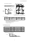
Input and output register
This product is provided with an input register and an output register so that the product can interface
with MPUs having speed differing from the internal operation.
Input register
The input register is a register that is used for temporarily storing the data to be written in the display
data RAM. The data to be written from the MPU to the input register will be automatically written in
the display data RAM through internal operation.
When the Chip Select is selected and R / W = 0, D / I =0, the data is written in the register,
synchronized with the fall of signal E.
Output register
The output register is a register that is used for temporarily storing the data to be read from the
display data RAM.