


www.ti.com
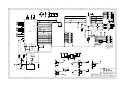
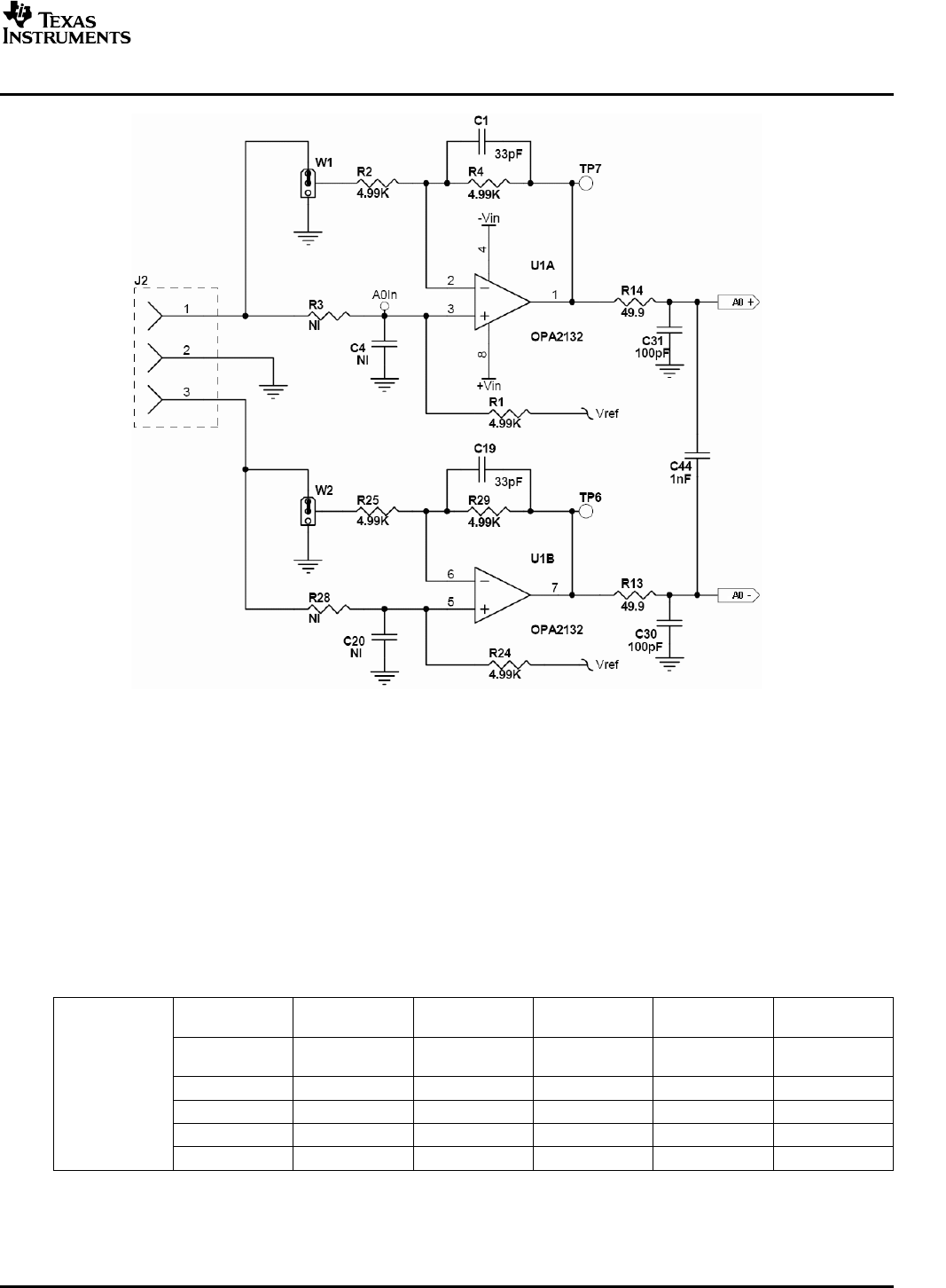
3.2BipolarInputtoChannelA0
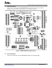
AnalogInterface
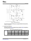
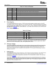
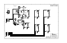
NOTE:ComponentsmarkedNIareNOTINSTALLED.
Figure1.ChannelA0InputCircuit
Thisconfigurationallowssingle-endedsignalsof±2.5V(+5Vpp)tobeappliedtoeitherinputofchannel
A0(J2pin1or3referencedtopin2).TheinputalsocanbeappliedtoconnectorJ4(notshown)pins2or
4,referencedtoanalogground.
Bychangingcomponentsandsettingtheappropriatejumper,itispossibletoconfiguretheinputbufferto
acceptbipolarinputvoltages.Table1isrelatedtotheschematicpresentedinFigure1andrepresentsjust
afewofthepossibleinputconfigurations.
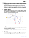
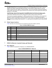
Table1.TypicalAnalogInputBufferCircuitValues
InputVoltageR3R2R1R4W2
R28R25R24R29W1
RefertoFigure1Defaultopen5kΩ5kΩ5kΩ1–2
0–+5
0–2.55kΩ5kΩopen5kΩ2–3
–2.5–+2.520kΩ4kΩ20kΩ4kΩ2–3
–5–+520kΩ4kΩ10kΩ2kΩ2–3
–10–+1020kΩ4kΩ5kΩ1kΩ2–3
SLAU189–September2006ADS8364/65MEVM3
SubmitDocumentationFeedback