


User's Guide
SLAU336–March 2011
DAC3484/DAC3482 EVM
Contents
1 Introduction .................................................................................................................. 2
1.1 Overview ............................................................................................................ 2
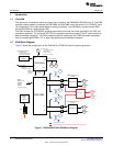
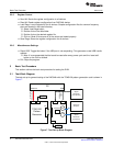
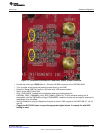
1.2 EVM Block Diagram ............................................................................................... 2
2 Software Control ............................................................................................................ 3
2.1 Installation Instructions ............................................................................................ 3
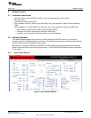
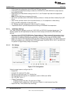
2.2 Software Operation ................................................................................................ 3
3 Basic Test Procedure ....................................................................................................... 8
3.1 Test Block Diagram ................................................................................................ 8
3.2 Test Set-Up Connection ........................................................................................... 9
3.3 TSW3100 Quick Start Operation ................................................................................. 9
3.4 DAC348x Software Quick Start Guide ......................................................................... 10
4 Optional Configuration .................................................................................................... 12
4.1 Configuring and Testing the DAC3484 Transformer Coupled Output ..................................... 12
4.2 Using the DAC3482 or Configuring DAC3484 in DAC3482 mode ......................................... 15
List of Figures
1 DAC3484/DAC3482 EVM Block Diagram ............................................................................... 2
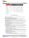
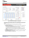
2 Input Control Options....................................................................................................... 3
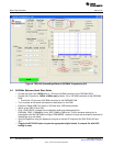
3 PLL Configuration........................................................................................................... 4
4 Digital Block Options ....................................................................................................... 5
5 Output Control Options..................................................................................................... 6
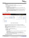
6 CDCE62005 Tab Configured for 4x Interpolation....................................................................... 7
7 Test Set-up Block Diagram ................................................................................................ 8
8 TSW3100 CommsSignalPattern (WCDMA) Programming GUI ..................................................... 10
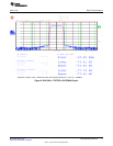
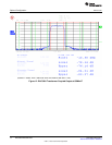
9 DAC3484 + TRF3703-15 WCDMA Output ............................................................................ 11
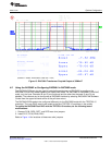
10 DAC3484 + TRF3703-15 WCDMA Output ............................................................................ 12
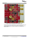
11 Locations of DAC348x to Transformer Output Jumper Locations .................................................. 13
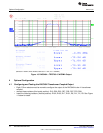
12 DAC3484 Transformer Coupled Output at 60MHz IF ................................................................ 14
13 DAC3484 Transformer Coupled Output at 30MHz IF ................................................................ 15
14 Locations of the DAC3482 to TRF3703-15 Interface Jumpers...................................................... 16
15 TSW3100 GUI Configuration for Generating a WCDMA Signal for DAC3482 .................................... 17
1
SLAU336–March 2011 DAC3484/DAC3482 EVM
Submit Documentation Feedback
© 2011, Texas Instruments Incorporated