


CONFIDENTIAL – DO NOT COPY
Page 8-12
File No. SG-0184
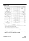
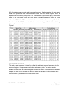
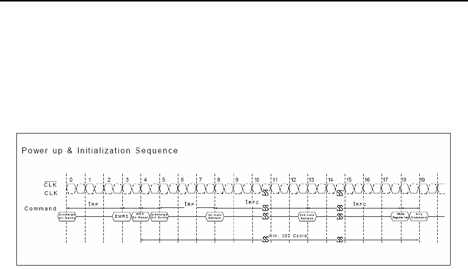
6. Issue a mode register set command for “DLL reset”. The additional 200 cycles of clock input
is required to lock the DLL.(To issue DLL reset command, provide “High” to A8 and “Low” to
BA0)
7. Issue precharge commands for all banks of the device.
8. Issue 2 or more auto-refresh commands.
9. Issue a mode register set command with low to A8 to initialize device operation.
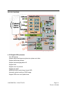
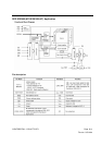
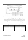
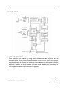
2. Mode Register Set (MRS)
The mode register stores the data for controlling the various operating modes of DDR SDRAM.
It programs CAS latency, addressing mode, burst length, test mode, DLL reset and various
vendor specific options to make DDR SDRAM useful for variety of different applications. The
default value of the register is not defined, therefore the mode register must be written after
EMRS setting for proper DDR SDRAM operation. The mode register is written by asserting low
on CS , RAS , CAS , WE and BA0 (The DDR SDRAM should be in all bank recharge with CKE
already high prior to writing into the mode register). The state of address pins A0~A11 in the
same cycle as CS , RAS , CAS , WE and BA0 going low is written in the mode register. Two
clock cycles are requested to complete the write operation in the mode register. The mode
register contents can be changed using the same command and clock cycle requirements
during operation as long as all banks are in the idle state. The mode register is divided into
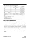
various fields depending on functionality. The burst length uses A0~A2, addressing mode uses
A3, CAS latency (read latency from column address) uses A4~A6. A7 is used for test mode.
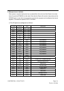
A8 is used for DLL reset. A7 must be set to low for normal MRS operation. Refer to the table
for specific codes for various burst length, addressing modes and CAS latencies.