


MAX5811
optocouplers to interface directly to the device. The
digital inputs are compatible with CMOS logic levels.
Power-Supply Bypassing and
Ground Management
Careful PC board layout is important for optimal system
performance. Keep analog and digital signals separate
to reduce noise injection and digital feedthrough. Use a
ground plane to ensure that the ground return from
GND to the power-supply ground is short and low
impedance. Bypass V
DD
with a 0.1µF capacitor to
ground as close to the device as possible.
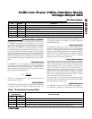
Chip Information
TRANSISTOR COUNT: 7172
PROCESS: BiCMOS
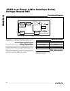
10-Bit Low Power 2-Wire Interface Serial,
Voltage-Output DAC
12 ______________________________________________________________________________________
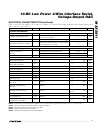
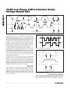
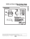
10-BIT
DAC
INPUT
REGISTER
MUX AND DAC
REGISTER
RESISTOR
NETWORK
POWER-DOWN
CIRCUITRY
SERIAL
INTERFACE
V
DD
SDA ADD SCL GND
OUT
MAX5811
Functional Diagram
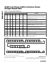
Selector Guide
PART ADDRESS
MAX5811LEUT 0010 00X
MAX5811MEUT 0010 01X
MAX5811NEUT 0110 10X
MAX5811PEUT 1010 10X