


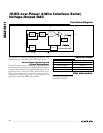

MAX5811
10-Bit Low Power 2-Wire Interface Serial,
Voltage-Output DAC
_______________________________________________________________________________________ 3
Note 1: All devices are 100% production tested at T
A
= +25°C and are guaranteed by design for T
A
= T
MIN
to T
MAX
.
Note 2: Static specifications are tested with the output unloaded.
Note 3: Linearity is guaranteed from codes 29 to 995.
Note 4: Offset and gain error limit the FSR.
Note 5: Guaranteed by design. Not production tested.
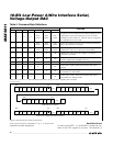
ELECTRICAL CHARACTERISTICS (continued)
(V
DD
= +2.7V to +5.5V, GND = 0, R
L
= 5kΩ, C
L
= 200pF, T
A
= T
MIN
to T
MAX
, unless otherwise noted. Typical values are at
V
DD
= +5V, T
A
= +25°C.) (Note 1)
PARAMETER
SYMBOL
CONDITIONS
MIN TYP MAX
UNITS
DYNAMIC PERFORMANCE
Voltage-Output Slew Rate SR 0.5
V/µs
Voltage-Output Settling Time
To 1/2LSB code 100 hex to 300 hex or 300
hex to 100 hex (Note 5)
412µs
Digital Feedthrough
Code = 000 hex, digital inputs from 0 to V
DD
0.2
nV-s
Digital-to-Analog Glitch Impulse
Major-carry transition (code = 1FF hex to 200
hex and 200 hex to 1FF hex)
12
nV-s
POWER SUPPLIES
Supply Voltage Range V
DD
2.7 5.5 V
All digital inputs at 0 or V
DD
= 3.6V
100 170
Supply Current with
No Load
All digital inputs at 0 or V
DD
= 5.5V
130 190
Power-Down Supply Current All digital inputs at 0 or V
DD
= 5.5V 0.3 1 µA
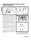
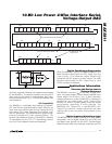
TIMING CHARACTERISTICS (Figure 1)
Serial Clock Frequency f
SCL
0
400
kHz
Bus-Free Time Between STOP
and START Conditions
t
BUF
1.3 µs
START Condition Hold Time
t
HD
,
STA
0.6 µs
SCL Pulse Width Low t
LOW
1.3 µs
SCL Pulse Width High t
HIGH
0.6 µs
Repeated START Setup Time
t
SU
,
STA
0.6 µs
Data Hold Time
t
HD
,
DAT
0 0.9 µs
Data Setup Time
t
SU
,
DAT
100
ns
SDA and SCL Receiving
Rise Time
t
r
(Note 5) 0
300
ns
SDA and SCL Receiving
Fall Time
t
f
(Note 5) 0
300
ns
SDA Transmitting Fall Time t
f
(Note 5)
20 +
0.1C
b
250
ns
STOP Condition Setup Time
t
SU
,
STO
0.6 µs
Bus Capacitance C
b
(Note 5)
400
pF
Maximum Duration of
Suppressed Pulse Widths
t
SP
050ns