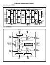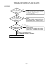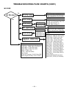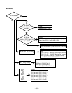
SCHEMATIC DIAGRAMS
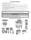
NOTES ON SCHEMATIC DIAGRAMS
1. All resistance values in ohms K=1,000 M=1,000,000.
2. Unless otherwise noted on schematic, all capacitor values less than 1 are expressed in µF (Micro Farad), and
the values more than 1 are in pF.
3. Unless otherwise noted on schematic, voltage reading taken with VOM from point indicated to chassis
ground. Voltage reading taken using color-bar signal VHF channel 5, all controls at normal. Line voltage at 120
volts. Some voltages may vary with signal strength.
4. Waveforms were taken with color-bar signal and controls set for normal picture. Waveforms marked with an
✽ may vary with signal strength.
5. The Symbol indicates a fusible resistor, which protects the circuit from possible short circuits.
— 42 —
SERVICE NOTES:
1. When replacing parts on circuit boards, clamp the lead wires to terminals before soldering.
PRODUCT SAFET
Y NOTICE
THE COMPONENTS DESIGNATED BY A STAR (★) ON THIS SCHEMATIC DIAGRAM DESIGNATE COMPONENTS
WHOSE VALUES ARE OF SPECIAL SIGNIFICANCE TO PRODUCT SAFETY. SHOULD ANY COMPONENT
DESIGNATED BY A STAR NEED TO BE REPLACED, USE ONLY THE PART DESIGNATED IN THE PARTS LIST. DO NOT
DEVIATE FROM THE RESISTANCE,WATTAGE AND VOLTAGE RATINGS SHOWN.
1
1
1
1
TOP VIEW
SIDE VIEW
COUNT TERMINALS IN
ARROW DIRECTION
MARK
E
C
B
AK
A
K
AK
A
K
A
K
A
K
INFRARED EMITTING
A....ANODE
K....CATHODE
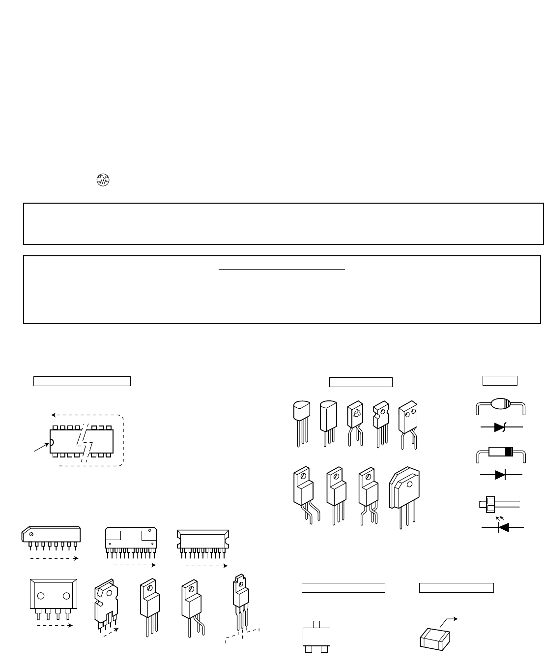
INTEGRATED CIRCUITS
TRANSISTORS
1
DIODES
PHOTO COUPLERS
B ... BASE
C ... COLLECTOR
E ... EMITTER
E
C
B
E
C
B
EC
B
EC
B
E
C
B
E
C
B
E
C
B
E
C
B
3
2
1
3
2
1
GND
(2)
IN
(1)
OUT
(3)
1 1
TOP VIEW
1
CHIP TRANSISTORS
B
C
E
TOP VIEW
B ... BASE
C ... COLLECTOR
E ... EMITTER
CHIP RESISTORS
TOP VIEW
123
12 x 10 = 12K ohm
3
IC, DIODE, AND TRANSISTOR PIN LAYOUTS


