


CONFIDENTIAL – DO NOT COPY
Page 7-16
File No. SG-0198
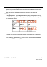
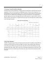
7.Precharge Timing During Write Operation
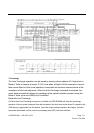
Precharge timing for Write operations in DRAMs requires enough time to satisfy the write recovery
requirement. This is the time required by a DRAM sense amp to fully store the voltage level. For
DDR SDRAMs, a timing parameter (tWR) is used to indicate the required amount of time between
the last valid write operation and a Precharge command to the same bank. The “write recovery”
operation begins on the rising clock edge after the last DQS edge that is used to strobe in the last
valid write data. “Write recovery” is complete on the next 2nd rising clock edge that is used to strobe
in the Precharge command.
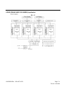
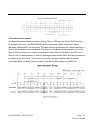
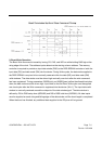
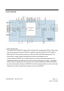
8. Burst Stop Command
The Burst Stop command is valid only during burst read cycles and is initiated by having RAS and
CAS high with CS and WE low at the rising edge of the clock. When the Burst Stop command is
issued during a burst Read cycle, both the output data (DQ) and data strobe (DQS) go to a high
impedance state after a delay (LBST) equal to the CAS latency programmed into the device. If the
Burst Stop command is issued during a burst Write cycle, the command will be treated as a NOP
command.