


HSC-ADC-EVALC
Rev. 0 | Page 2 of 32
TABLE OF CONTENTS
Features.............................................................................................. 1
Equipment Needed........................................................................... 1
Product Highlights........................................................................... 1
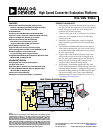
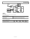
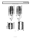
Functional Block Diagram .............................................................. 1
Revision History ............................................................................... 2
Product Description......................................................................... 3
Evaluation Board Description......................................................... 3
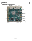
Evaluation Board Hardware............................................................ 4
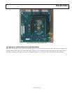
HSC-ADC-EVALC ADC Capture Board Easy Start............... 4
Power Supplies.............................................................................. 4
Connection and Setup .................................................................4
Jumpers.......................................................................................... 5
HSC-ADC-EVALC ADC Capture Board Features.................. 6
HSC-ADC-EVALC Supported ADC Evaluation Boards........ 7
Theory of Operation.........................................................................8
Configuration ................................................................................8
Input Circuitry...............................................................................8
Data Capture..................................................................................8
Code Description..........................................................................8
FPGA Configuration and Customization..................................8
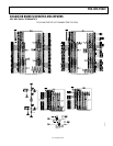
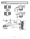
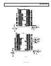
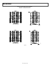
Evaluation Board Schematics and Artwork...................................9
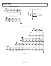
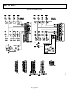
HSC-ADC-EVALC Schematics...................................................9
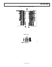
PCB Layout ................................................................................. 23
I/O Connector—J1, J2, and J3 Pin Mapping .......................... 24
Ordering Information.................................................................... 28
Bill of Materials (RoHS Compliant) ........................................ 28
Ordering Guide .......................................................................... 30
ESD Caution................................................................................ 30
REVISION HISTORY
4/07—Revision 0: Initial Version