


HSC-ADC-EVALC
Rev. 0 | Page 3 of 32
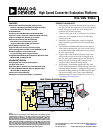
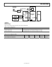
PRODUCT DESCRIPTION
The Analog Devices, Inc. high speed converter evaluation
platform (HSC-ADC-EVALC) includes the latest version of
VisualAnalog and an FPGA-based buffer memory board to capture
blocks of digital data from the Analog Devices high speed
analog-to-digital converter (ADC) evaluation boards. The ADC
capture board is connected to the PC through a USB port and is
used with VisualAnalog to quickly evaluate the performance of
high speed ADCs. Users can view an FFT for a specific analog
input and encode rate to analyze SNR, SINAD, SFDR, and
harmonic information.
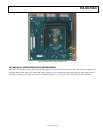
The ADC capture board is easy to set up. Additional equipment
needed includes an Analog Devices high speed ADC evaluation
board, a signal source, and a clock source. Once the kit is
connected and powered, the evaluation is enabled instantly on
the PC.
The ADC capture board enables numerous expansion and
evaluation possibilities by virtue of its powerful reconfigurable
FPGA core.
The system can acquire digital data at speeds up to 644 MSPS
single data rate (SDR) and 800 MSPS double data rate (DDR).
The FPGA contains an integrated FIFO memory that allows
capture of data record lengths up to a total of 64 kB. A USB 2.0
microcontroller communicating with VisualAnalog allows
for easy interfacing to newer computers using the USB 2.0
(USB 1.1 compatible) interface.
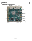
EVALUATION BOARD DESCRIPTION
The ADC capture board provides all of the support circuitry
required to accept two 18-bit channels from an ADC’s parallel
CMOS or LVDS outputs. Various functions such as FPGA
configuration load options and I/O logic levels can be selected by
proper connection of various jumpers or switches (see
Table 1).
When using the HSC-ADC-EVALC in conjunction with an
ADC evaluation board, it is critical that the signal sources used
for the ADC board’s analog input and clock have very low phase
noise (<1 ps rms jitter) to achieve the ultimate performance of
the converter.
Proper filtering of the analog input signal to remove harmonics
and lower the integrated or broadband noise at the input is also
necessary to achieve the specified noise performance.
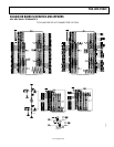
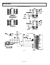
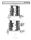
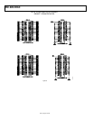
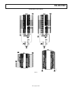
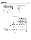
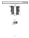
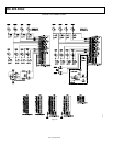
See
Figure 5 to Figure 20 for complete schematics and layout plots.