


14
5.2 Function Specifications
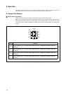
Table 5.2 lists the function specifications of the header board.
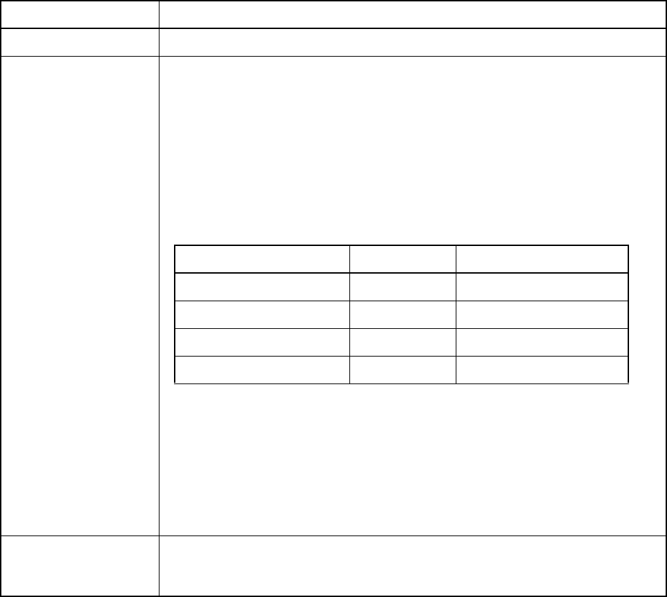
Table 5.2 Function Specifications of Header Board
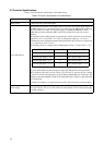
Item Specification
Header board Connects the user system and adapter.
Level shift function
The header board includes a level shifter used to convert the VCC5 level output signals of
the MB91V460 or user system to the VCC3 level when using the MB91V460 (evaluation
MCU: user I/O uses a single VCC5 power supply) to emulate an MB91461 or other
MB91460 series mass production MCU (user I/O uses dual VCC5 and VCC3 power
supplies) .
The potential of level-shifted signals corresponding to VCC5 and VCC3 are in the range
upper limit = 4.4 V, lower limit = 3 V (error for each power supply is ± 1 V or less) .
Note that the circuit configuration means that I/O pins that expect VCC5 level signals will
have a signal level of 4.4 V or less.
The following shows an example of level shifting when VCC5 = 5 V and VCC3 = 3.3 V.
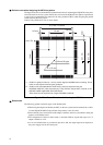
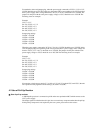
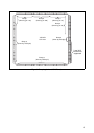
The level shift function separates the power supply pins that drive the mass production
MCU's I/O pins (VCC3 pin, pin 133 (VCC5) , pin 147 (VCC5) , pin 162 (VCC5) , and pin
176 (VCC5) ) into five groups and sets up level shifting independently for each group. The
settings are specified using the VCCB1 to VCCB5 jumper plugs. Figure 5.1 shows the make
up of each group.
Note that level shifting is not performed for pins 89 to 108 on the mass production MCU.
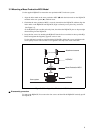
Power supply
Selects the power supply with different potential to VCC3 among the MB91461’s VCC5
pins (pin 176, 162, 147, or 133) and connects it to the adapter Use the VCC5 jumper plug
to set this selection.
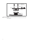
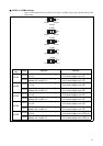
MB91V460 Level Shift Mass Production MCU
VCC5 I/O pin output = 5 V → VCC5 I/O pin input = 4.4 V
VCC5 I/O pin output = 5 V → VCC3 I/O pin input = 3.3 V
VCC5 I/O pin input = 4.4 V ← VCC5 I/O pin output = 5 V
VCC5 I/O pin input = 3.3 V ← VCC3 I/O pin output = 3.3 V