


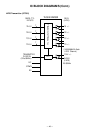
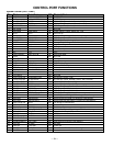
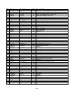
— 54 —
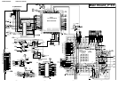
Pin Name Function I/O Description
1 VHOLD VHOLD at CAPTION IN CAPTION
2 HLF HLF at CAPTION IN CAPTION
3 DA1/SCL3/RXD2 IIC SCL OUT IIC Bus SCL (Tuner, Audio Control, AV SW)
4 DA0/SDA3/TXD2 IIC SDA I/O IIC Bus SDA (Tuner, Audio Control, AV SW)
5 TB2IN/DIGR0 OSD RED 0 OUT OSD Output Red (Low level)
6 P91/TB1IN – – Not used
7 P90/TB0IN PWR SW IN IN Power ON/OFF Detect, Switch On : Low
8 BYTE BYTE IN 3.3V Pull Up
9 CNVss IN Normal : Low, Writing to Flash Memory : High
10 Xcin/DIGG0 OSD GREEN 0 OUT OSD Output Green (Low level)
11 Xcout/DIGB0 OSD BLUE 0 OUT OSD Output Blue (Low level)
12 RESET RESET 3.3V IN Normal : 3.3V, Writing to Flash Memory : Low -> 3.3V
13 Xout Main Clock Output
14 Vss GND GND
15 Xin Main Clock Input
16 Vcc 3.3V 3.3V
17 OSC1/OSCHLF OSD_CLK_IN IN OSD Clock Input
18 OSC2 OUT Not used
19 P83/INT1 RC IN RC Input
20 P82/INT0 OUT Not used
21 OUT1 OSD_BLK OUT OSD Blanking Output
22 OUT2 OSD-HALF OUT OSD Half Tone Output
23 P77/HC1 OUT Not used
24 P76/TA3OUT FAN CONTROL PWM Not used
25 P75/HC0 IN Not used
26 P74/TA2out OUT Not used
27 P73/CTS2/RTS2 NV MEMORY SW OUT NV Memory Access : High
28 P72/SCL2/CLK2 IIC SCL/SCLK OUT IIC Bus SCL (Panel, Decoder, Scaler, A/D Converter)
29 P71/SCL1/RXD2 IIC SCL I/O IIC Bus SCL (N.V., Factory PC)
30 P70/SDA1/TXD2 IIC SDA OUT IIC Bus SDA (N.V., Factory PC)
31 P67/SDA2 IIC SDA/SDATA I/O IIC Bus SDA (Panel, Decoder, Scaler, A/D Converter)
32 R/DIGR1 OSD RED output OUT OSD Output Red (Middle level)
33 G/DIGR1 OSD GREEN output OUT OSD Output Green (Middle level)
34 B/DIGR1 OSD BLUE output OUT OSD Output Blue (Middle level)
35 P63/TxD0 DM SOUT/TXD OUT Serial Output to US Digital, For writing to Flash Memory
36 P62/RxD0 DM SIN/RXD IN Serial Input to US Digital, For writing to Flash Memory
37 P61/CLK0 DM CLK/SCLK IN Serial Clock from US Digital, For writing to Flash Memory
38 P60/CTS0/RTS0 BUSY OUT For writing to Flash Memory
39 P57/RDY/CLKout IN Not used
40 P56/ALE STATUS IN For factory Status
41 P55/HOLD PULL-DOWN GND Pull down to Ground, For writing to EPM Flash Memory
42 P54/HLDA DM_OUT OUT Digital Module Output (CS)
43 P53/BCLK AV SW4 OUT AV SW4
44 P52/RD AV SW3 OUT AV SW3
45 P51/WRH/BHE OUT Not used
46 P50/WRL/WR/CE Clip Enable OUT Chip Select for writing to Flash Memory
47 P47/CS3 AV SW2 OUT AV SW2
48 P46/CS2 LVDS SW OUT LVDS SW
49 P45/CS1 PWR_GO OUT Power Control TV-GO, Power ON : High
50 P44/CS0 OUT Not used
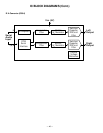
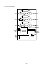
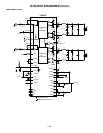
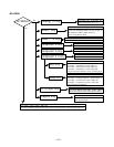
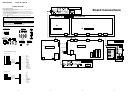
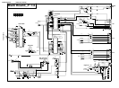
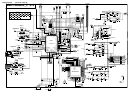
System Control (CPU : IC801)
CONTROL PORT FUNCTIONS