Overview
The
DV29
is effectively a no compromise version both
electronically and mechanically of the
DV79
.
The player is based around acclaimed Zoran Vaddis
V
chipset coupled to high specification
Wolfson
D to A
converters for all six audio output channels, also
featured in this design is a
HDMI
transmitter with
digital Video and a Audio output capable of Digital
Surround.
The DV29 and the DV79 use the same main board
and power supply stage but with many of the
components either upgrade or replaced with different
topologies, many of the critical audio/video
components with 0.1% tolerance within the DV29 and
we also have an extra toroid power supply for the
Audio stages.
Both the HDMI chip and Video encoder are of a higher
quality than those found inside the DV79.
Power supply board.
Non-switching
Mains power arrives at IEC inlet socket SKT1 and is
filtered by EMC choke LI and Y caps C3 and C4,
mains switch SW2a/b switches both Negative and Live
phases before the power reaches the mains select
switch at location
SW1
the switch allows the primary
windings of the transformer
TX1
to be wired in either
Parallel or Series configuration.
The Bridge rectifying Diode package at location
D1
forms the basis of the conventional power stage and
supplies a VN35V6 (-35.6v) to the Switch mode
stage, transistor
TR1
is biased by 2v7 Zener diode
DZ1
and allows for the series Zener diodes
DZ2, DZ3,
DZ3
to supply the VN13V5 and VN19V rails.
We will also see a simple
A.C present circuit
this is
used for delayed output relay operation and fast relay
closure under interrupted supply conditions thus
preventing op-amp offsets from reaching the Audio
output sockets.
Switch mode
The switch mode supply is formed around the
Driver/Control chip
IC1
UC3843 (used in regulating
mode). The chip is referenced the –36.5V supply line
and the Digital ground DGND, the supply for the chip
is formed by the 12v Zener at location
DZ6
and can be
seen on Pin 7 as VCC. The power supply allows for
the switch-mode to be tied the to Audio sampling
frequency for any given compatible format see Fig 1.
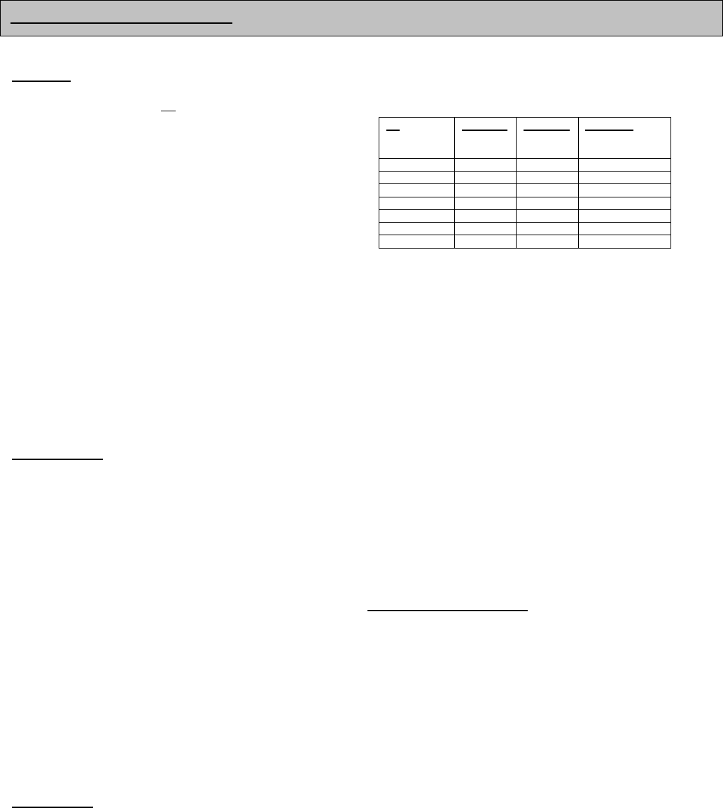
Fig 1 PSU clock control and IC305 line status
Fs
Frequency
select
PSUFS1
Pin 11
IC305a
PSUFS0
Pin 12
IC305a
PSUCLK
Output Pin 5
of IC305a
44.1 kHz 0 0 44.1 kHz
48 kHz 0 0 48 kHz
88.2 kHz 0 1 44.1kHz
96 kHz 0 1 48 kHz
176.4 kHz 1 0 44.1 kHz
192 kHz 1 0 48 kHz
Others 1 1 OFF
The
PSU sync signal
is driven into the power supply via
Resistor R9 if no Sync is present the unit is set to free run at
xxxx due to the RT/RC network attached to Pin 4.
IC1
is running in regulated mode and monitors the voltage
output on the +5V and +3V3 D.C lines, the two voltages are
summed by
TR8
and Driven into the VFB and Comp inputs
of IC1, the Voltage is then regulated by changing the time
base of the PWM output at pin 6 (longer the time base the
lower the voltage), the
PWM switching frequency
is driven
into the switch-mode transformer by the high speed Nmos
device at position M1, R5 is used to sense the Current
across the gate of the Nmosfet and in the event of a short
circuit will safely shut the power supply down. We derive the
12v Mech supply from the output of M1 using the Ultra-fast
Diode at location D8 to rectify the PWM line.
The D.C outputs from the switch mode have extensive
switch mode noise removing filters these are seen as 100n
caps down to ground and Wire wound inductors in series
with the supply rail.
Power supply main board
All the power supply rails are supplied to the main board via
the 32 way FFC conector at location
CON1001
.
The Digital supplies from the switch mode stage of the
power supply arrive as
3V3D
,
+5VD
and
+12VD
we also see
the Display board power supplies arrive as
–19V
,
-9V
and
–13.5V
all of the supplies have a second stage of
implemented on the board to remove all traces of ultra-sonic
noise.
The 3V3D rail is the main 3V3 rail used to power the digital
circuitry; +5VD is used for all 5v Digital/Video supplies the
+12VD is used for Scart switching and to power the HDMI
circuit (not DV78).
The 1V8 rail is derived from the 3V3 rail and is regulated by
the adjustable regulator at location
REG1003
.
FMJ Dv29 Circuit description.


