


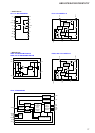
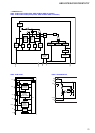


HBD-E370/E470/E570/E870/T57
79
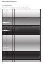
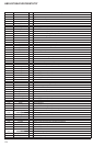
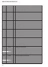
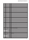
Pin No. Pin Name I/O Description
J9 DVSS - Ground terminal
J11 DVSS - Ground terminal
J13 DVSS - Ground terminal
J15 VCC3IO_3 - Power supply terminal (+3.3V)
J17 VIND9 - Not used
J19 DVSS - Ground terminal
J21 VCC3IO_PWM - Power supply terminal (+3.3V)
J23 DVSS - Ground terminal
J25 AVSS12_27MPLL - Ground terminal
J27 AVDD33_HDMI - Power supply terminal (+3.3V)
J29 AVSS12_HDMI - Ground terminal
J33 VCC3IO_STB - Power supply terminal (+3.3V)
J37 AVDD33_LDO - Power supply terminal (+3.3V)
J39 SFCS O Chip select signal output to the serial fl ash
J41 NFD1 I/O Two-way data bus with the NAND fl ash
J43 NFD2 I/O Two-way data bus with the NAND fl ash
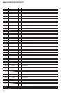
K2 FE_MPXOUT2 O Digital audio data output terminal for the SACD
K4 FE_EQBIAS - Not used
K6 FE_SFCS# O Chip select signal output terminal for the front-end serial fl ash
K8 NS_RFIP I SACD audio data (positive) input terminal
K34 DVSS - Ground terminal
K36 AVSS33_LDO - Ground terminal
K38 NFCLE O Command latch enable signal output to the NAND fl ash
K40 NFD3 I/O Two-way data bus with the NAND fl ash
K42 NFD4 I/O Two-way data bus with the NAND fl ash
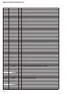
L1 FE_VWDC3O - Not used
L3 FE_VDAC0 - Not used
L5 FE_MPXOUT1 O Digital audio data output terminal for the SACD
L7 FE_SFWP# - Not used
L9 FE_GIO8 - Not used
L35 VCC3IO_2 - Power supply terminal (+3.3V)
L37 NFALE O Address latch enable signal output to the NAND fl ash
L39 NFCEN2 O Chip enable signal output terminal Not used
L41 NFD5 I/O Two-way data bus with the NAND fl ash
L43 NFD6 I/O Two-way data bus with the NAND fl ash
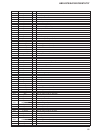
M2 FE_VWDC2O - Not used
M4 FE_AUX1 I Monitoring signal input from the BD drive
M6 FE_RSTI I Reset signal input terminal for the front-end power
M8 FE_MVDDO - Power supply terminal (+3.3V)
M10 FE_MVDDO - Power supply terminal (+3.3V)
M36 NFREN O Read enable signal output to the NAND fl ash
M38 NFCEN O Chip enable signal output to the NAND fl ash
M40 NFD7 I/O Two-way data bus with the NAND fl ash
M42 B_REXTDN - Not used
N1 FE_INB O Main beam (B) input from the BD drive
N3 FE_TRINC - Not used
N5 FE_VFVREF - Not used
N7 FE_DVDD33O - Power supply terminal (+3.3V)
N9 FE_DVDD33O - Power supply terminal (+3.3V)
N11 FE_DVDD33O - Power supply terminal (+3.3V)
N35 VCC3IO_2 - Power supply terminal (+3.3V)
N37 DVSS - Ground terminal
N39 DVSS - Ground terminal
N41 B_RCLK1 O Clock signal (positive) output to the SD-RAM
N43 B_RCLK1B O Clock signal (negative) output to the SD-RAM
P2 FE_INA O Main beam (A) input from the BD drive
P4 FE_TRINA - Not used
P6 FE_VWDC1O - Not used
P8 FE_AVDD12_1 - Power supply terminal (+1.2V)
P10 FE_DVDD33O - Power supply terminal (+3.3V)