


HBD-E370/E470/E570/E870/T57
84
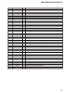
Pin No. Pin Name I/O Description
AK42 VCC2IO - Power supply terminal (+1.8V)
AL1 USB_DP0 I/O USB differential serial data (positive) input/output with the USB connector (rear side)
AL3 USB_DM1 I/O USB differential serial data (negative) input/output with the USB connector (front side)
AL5 AVSS33_USB - Ground terminal
AL7 FE_SVDD33 - Power supply terminal (+3.3V)
AL21 VCCK - Power supply terminal (+1.1V)
AL23 VCCK - Power supply terminal (+1.1V)
AL25 VCCK - Power supply terminal (+1.1V)
AL27 VCCK - Power supply terminal (+1.1V)
AL29 VCCK - Power supply terminal (+1.1V)
AL31 VCCK - Power supply terminal (+1.1V)
AL35 VCC2IO - Power supply terminal (+1.8V)
AL37 B_RDQ11 I/O Two-way data bus with the SD-RAM
AL39 B_RDQ14 I/O Two-way data bus with the SD-RAM
AL41 B_RCLK0B O Clock signal (negative) output to the SD-RAM
AL43 B_RCLK0 O Clock signal (positive) output to the SD-RAM
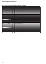
AM2 USB_DP1 I/O USB differential serial data (positive) input/output with the USB connector (front side)
AM4 USB_VRT - Not used
AM6 FE_SXVDD33 - Power supply terminal (+3.3V)
AM8 FE_TLO O Motor drive signal output to the motor driver IC
AM36 B_RDQM1 O Data mask signal output to the SD-RAM
AM38 B_RDQ12 I/O Two-way data bus with the SD-RAM
AM40 B_RDQ10 I/O Two-way data bus with the SD-RAM
AM42 B_RDQ13 I/O Two-way data bus with the SD-RAM
AN1 FE_STXP O SATA channel 1 RX differential pair signal (positive) output terminal
AN3 AVDD33_USB - Power supply terminal (+3.3V)
AN5 FE_SAGND - Ground terminal
AN7 FE_SPLLVDD12 - Power supply terminal (+1.2V)
AN35 DVSS - Ground terminal
AN37 DVSS - Ground terminal
AN39 DVSS - Ground terminal
AN41 B_RDQ15 I/O Two-way data bus with the SD-RAM
AN43 B_RDQ8 I/O Two-way data bus with the SD-RAM
AP2 FE_STXN O SATA channel 1 RX differential pair signal (negative) output terminal
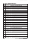
AP4 CORE_RESETB I System reset signal input from the system controller
AP6 FE_STXVDD12 - Power supply terminal (+1.2V)
AP8 FE_AVDD12_RX - Power supply terminal (+1.2V)
AP36 B_RDQ7 I/O Two-way data bus with the SD-RAM
AP38 B_RDQM0 O Data mask signal output to the SD-RAM
AP40 VCC2IO - Power supply terminal (+1.8V)
AP42 VCC2IO - Power supply terminal (+1.8V)
AR1 FE_SRXP I SATA channel 1 TX differential pair signal (positive) input terminal
AR3 FE_SRXN I SATA channel 1 TX differential pair signal (negative) input terminal
AR5 RTCRBIAS - Not used
AR7 AVDD12_ADC - Power supply terminal (+1.2V)
AR17 DVSS - Ground terminal
AR19 VCC2IO - Power supply terminal (+1.8V)
AR25 DVSS - Ground terminal
AR29 DVSS - Ground terminal
AR31 VCC2IO - Power supply terminal (+1.8V)
AR37 B_RDQ6 I/O Two-way data bus with the SD-RAM
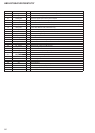
AR39 B_RDQ0 I/O Two-way data bus with the SD-RAM
AR41 B_RDQS1B O Data strobe signal (negative) output to the SD-RAM
AR43 B_RDQS1 O Data strobe signal (positive) output to the SD-RAM
AT2 XI_RTC I Not used
AT4 XO_RTC O Not used
AT6 AVSS12_ADC - Ground terminal
AT10 FE_GIO13 - Not used
AT12 SCL I/O Two-way clock bus with the EEPROM
AT14 DVSS - Ground terminal