33
Low Voltage Power supply
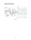
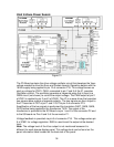
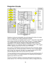
VCC and Start-up voltage for the low voltage power supply is provided to IC650
of the P5 Board by the standby power supply circuit (not shown). Upon start-up
of the switching control circuit, a pulse width modulated signal is output at pin 9
of connector P18/P18A to drive the switching transistor Q416. When Q416 is on,
current flows via the primary winding of transformer T401 and Q416. As current
flows through the transformer, energy is built up and stored in the transformer.
When Q416 turns off, the energy within the transformer begins to collapse. As
the field collapses, energy is released in the windings of the transformer to
provide the secondary voltages.
The rectified AC output at pin 10 of transformer T401 is applied to IC401 where it
is regulated to 18V. This voltage is used to power the Drive Oscillator circuit
board that will be discussed later.
Voltage Regulation
The 13.5V source and the VDA source voltage levels are monitored by IC650 of
the P5 Board. A voltage increase of the 13.5V or an increase in the current flow
of the VDA source causes IC416 to conduct harder, allowing more current to flow
through the LED inside opto-coupler D432. This increases the conduction of the
transistor inside D432. Conversely, a decrease in the 13.5V supply voltage or a
decrease in the current flow of the Vda source decreases the conduction of
IC416. Any change in the conduction of IC416 is monitored by pin 10 of IC450.
As a result, the pulse width modulated output at pin 10 of IC650 adjusts to keep
the output level of the power supply constant. R545 is used to adjust Vda to the
proper voltage level.


