34
High Voltage Power Supply
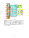
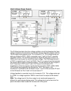
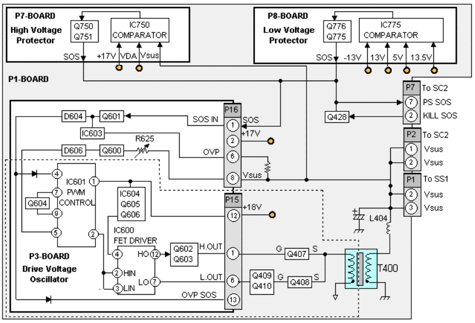
Figure 31
The P3-Board contains the drive voltage oscillator circuit that develops the Vsus
voltage needed to drive the Scan and Sustain boards. Operation begins with the
18Vdc supply being applied to pin 12 of connector P15. This voltage serves as
start up voltage for IC601. Q604, connected to pin 7 and 9 of the IC, provides
Oscillation control. The oscillator generates a trapezoid pulse that is input to a
PWM circuit (not shown) to control the output voltage. The PWM output at pin 2
of IC601 is applied to pin 2 and 3 of IC600. This IC is a wave driver that provides
two square wave outputs at opposite polarity. The two signals are then output to
the P1 board as H OUT at pin 1 and L OUT at pin 6 of connector P15.
Amplification of the two signals is performed the transistors Q407, Q408, Q409,
Q410 before being applied to the transformer T400. The output of the
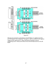
transformer is provided to the SC-Board via pin 1 and 2 of the connector P2 and
to the SS board via Pins 2 and 3 of the connector P1.
Voltage feedback is provided via pin 8 of connector P16. This voltage enters pin
5 of IC601 for voltage regulation. R625 is used to set the output at the desired
level.
Note: The voltage level of the Vsus output is not mentioned because it is
different for each plasma display panel. This voltage level can be found on the
panel information label located on the heat sink of the panel.


