Philips Semiconductors Product data sheet
SCC2691Universal asynchronous receiver/transmitter (UART)
2006 Aug 04
14
to placing the SCC2691 in this mode. Note that this bit must be set
to a logic 1 after reset.
When the power-down mode is enabled, internal circuitry forces the
X1/CLK pin to the low state and the X2 pin to the high state. If an
external clock is being used to drive the device, it is recommended
that the clock source be three-stated or forced low while the UART
is in power-down mode in order to prevent the clock driver from
being short circuited.
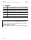
Table 5. BRG Characteristics
Nom Rate (Baud) Actual 16X Clock (kHz) Error (%)
50 0.8 0
75 1.2 0
110 1.759 –0.069
134.5 2.153 0.059
150 2.4 0
200 3.2 0
300 4.8 0
600 9.6 0
1050 16.756 –0.260
1200 19.2 0
1800 28.8 0
2000 32.056 0.175
2400 38.4 0
4800 76.8 0
7200 115.2 0
9600 153.6 0
14.4K 230.4 0
19.2k 307.2 0
28.8K 460.8 0
38.4k 614.4 0
57.6K 921.6 0
115.2K 1843.2K 0
Duty cycle of 16X clock is 50% ±1%. Crystal or Clock = 3.6864MHz
Asynchronous UART communications can tolerate frequency error
of 4.1% to 6.7% in a “clean” communications channel. The percent
of error changes as the character length changes. The above
percentages range from 5 bits not parity to 8 bits with parity and one
stop bit. The error with 8 bits no parity and one stop bit is 4.6%. If a
stop bit length of 9/16 is used, the error tolerance will approach 0
due to a variable error of up to 1/16 bit time in receiver clock phase
alignment to the start bit.
ACR[2:0] – MPO Output Select
This field programs the MPO output pin to provide one of the
following:
000 Request-to-send active-low output (RTSN). This output is
asserted and negated via the command register. RTSN
can be programmed to be automatically reset after the
character in the transmitter is completely shifted out or
when the receiver FIFO and receiver shift register are full
using MR2[5] and MR1[7], respectively.
001 The counter/timer output. In the timer mode, this output is
a square wave with a period of twice the value (in clock
periods) of the contents of the CTUR and CTLR. In the
counter mode, the output remains high until the terminal
count is reached, at which time it goes low. The output
returns to the high state when the counter is stopped by a
stop counter command.
010 The 1X clock for the transmitter, which is the clock that
shifts the transmitted data. If data is not being trans-
mitted, a non-synchronized 1X clock is output.
011 The 16X clock for the transmitter. This is the clock selected
by CSR[3:0] = 1111.
100 The 1X clock for the receiver, which is the clock that samples
the received data. If data is not being received, a non-syn-
chronized 1X clock is output.
101 The 16X clock for the receiver. This is the clock selected by
CSR[7:4], and is a 1X clock if CSR[7:4] = 1111.
110 The transmitter register empty signal, which is the comple-
ment of SR[2]. Active low output.
111 The receiver ready or FIFO full signal (complement of
ISR[2]). Active-low output.
ISR – Interrupt Status Register
This register provides the status of all potential interrupt sources. The
contents of this register are masked by the interrupt mask register
(IMR). If a bit in the ISR is a ‘1’ and the corresponding bit in the IMR
is also a ‘1’, the INTRN output is asserted (low). If the corresponding
bit in the IMR is a zero, the state of the bit in the ISR has no effect on
the INTRN output. Note that the IMR does not mask the reading of
the ISR; the true status is provided regardless of the contents of the
IMR. This register is cleared when the device is reset.
ISR[7] – MPI Change-of-State
This bit is set when a change-of-state occurs at the MPI input pin. It
is reset by a reset change interrupt command.
ISR[6] – MPI Current State
This bit provides the current state of the MPI pin. This information is
latched and reflects the state of the pin at the leading edge of the
ISR ready cycle.
ISR[4] – Counter Ready
In the counter mode of operation, this bit is set when the counter
reaches terminal count and is reset when the counter is stopped by
a stop counter command.
In the timer mode, this bit is set once each cycle of the generated
square wave (every other time the C/T reaches zero count). The bit
is reset by a stop counter command. The command, however, does
not stop the C/T.
ISR[3] – Change in Break
This bit, when set, indicates that the receiver has detected the
beginning or end of a received break. It is reset when the CPU
issues a reset break change interrupt command.
ISR[2] – Receiver Ready or FIFO Full
The function of this bit is programmed by MR1[6]. If programmed as
receiver ready, it indicates that a character has been received and is
waiting in the FIFO to be read by the CPU. It is set when the
character is transferred from the receive shift register to the FIFO
and reset when the CPU reads the receiver FIFO. If the FIFO
contains more characters, the bit will be set again after the FIFO is
read. If programmed as FIFO full, it is set when a character is
transferred from the receive holding register to the receive FIFO and
the transfer causes the FIFO to become full, i.e., all three FIFO
positions are occupied. It is reset when the FIFO is read and there is
no character in the receive shift register. If there is a character
waiting in the receive shift register because the FIFO is full, the bit is
set again when the waiting character is transferred into the FIFO.
ISR[1] – Transmitter Empty
This bit is a duplicate of TxEMT (SR[3]).
ISR[0] – Transmitter Ready
This bit is a duplicate of TxRDY (SR[2]).


