


Philips Semiconductors Product data sheet
SCC2691Universal asynchronous receiver/transmitter (UART)
2006 Aug 04
5
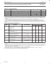
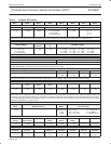
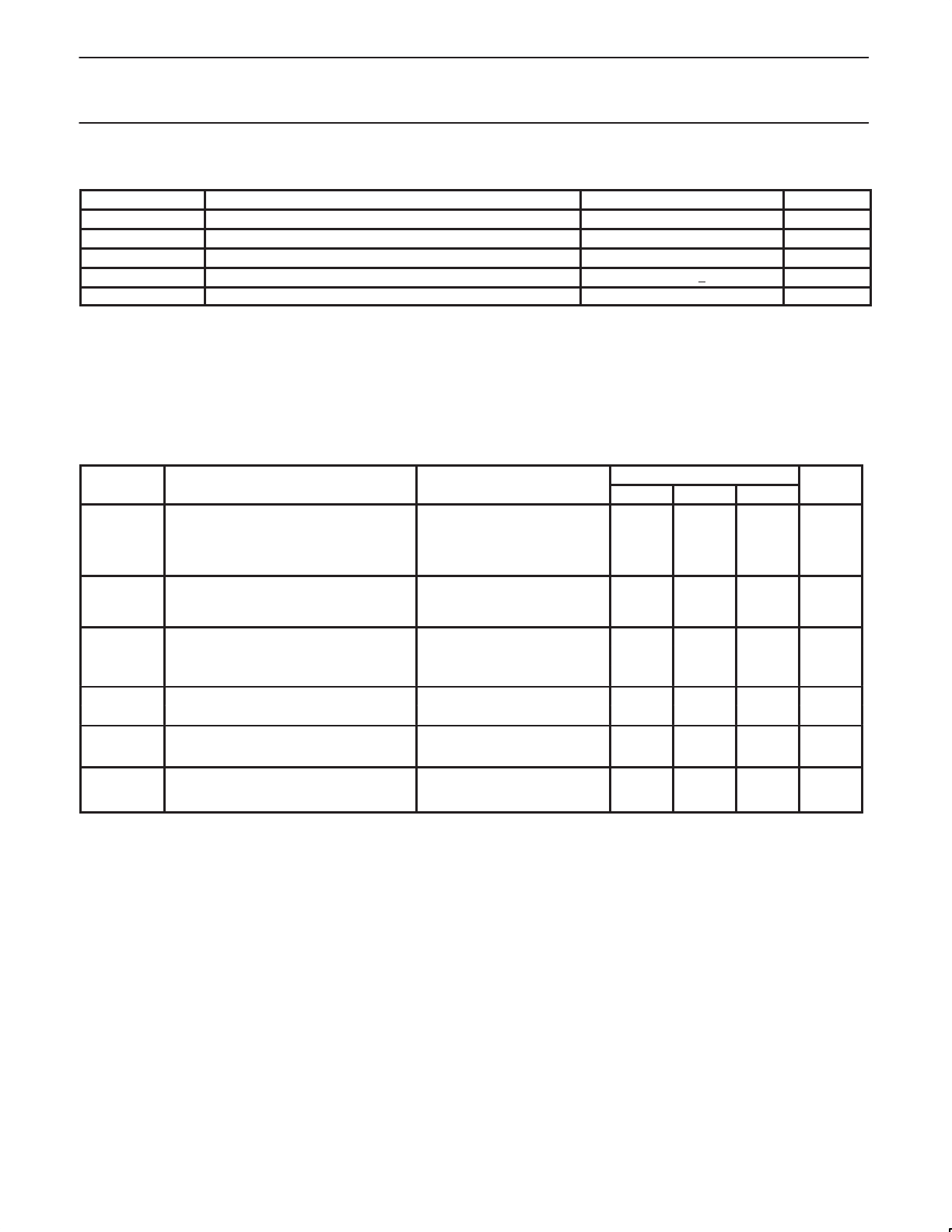
ABSOLUTE MAXIMUM RATINGS
1
SYMBOL
PARAMETER RATING UNIT
T
A
Operating ambient temperature range
2
Note 4 °C
T
STG
Storage temperature range –65 to +150 °C
V
CC
Voltage from V
CC
to GND
3
–0.5 to + 7.0 V
V
S
Voltage from any pin to ground
3
–0.5 to V
CC
+10% V
P
D
Power Dissipation 300 mW
NOTES:
1. Stresses above those listed under Absolute Maximum Ratings may cause permanent damage to the device. This is a stress rating only and
functional operation of the device at these or any other condition above those indicated in the operation section of this specification is not
implied.
2. For operating at elevated temperature, the device must be derated based on +150°C maximum junction temperature.
3. This product includes circuitry specifically designed for the protection of its internal devices from damaging effects of excessive static
charge. Nonetheless, it is suggested that conventional precautions be taken to avoid applying any voltages larger than the rated maxima.
4. Parameters are valid over specified temperature range. See Ordering Information table for applicable operating temperature and V
CC
supply
range.
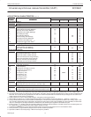
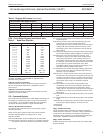
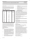
DC ELECTRICAL CHARACTERISTICS
1,
2,
3
SYMBOL
PARAMETER
TEST CONDITIONS
LIMITS
UNIT
SYMBOL
PARAMETER
TEST
CONDITIONS
Min Typ Max
UNIT
V
IL
V
IH
Input low voltage
Input high voltage
0.8 V
All except X1/CLK
X1/CLK
2
0.8V
CC
V
CC
V
V
V
OL
V
OH
4
Output low voltage
Output high voltage
(except open drain outputs)
I
OL
= 2.4mA
I
OH
= –400µA
2.4
0.4 V
V
I
IL
Input leakage current V
IN
= 0 to V
CC
–10 10 µA
I
LL
Data bus 3-State leakage current V
O
= 0.4 to V
CC
–10 10 µA
I
OD
Open-drain output leakage current V
O
= 0.4 to V
CC
–10 10
µA
I
XIL
X1/CLK low input current V
IN
= 0, X2 floated –100 –30 0 µA
I
XIH
X1/CLK high input current V
IN
= V
CC
, X2 floated 0 30 100 µA
I
X2L
X2 low output current V
OUT
= 0, X1/CLK = V
CC
–100 µA
I
X2H
X2 high output current V
OUT
= V
CC
, X1/CLK = 0V 100 µA
I
CCA
I
CCD
Power supply current, active
Power down current
5
0°C to +70°C
–40°C to +85°C
0.8
1.0
2.0
2.5
500
mA
mA
µA
NOTES:
1. Parameters are valid over specified temperature range. See Ordering Information table for applicable operating temperature and V
CC
supply
range.
2. All voltage measurements are referenced to ground (GND). For testing, all input signals swing between 0V and 3.0V with a transition time of
20ns max. For X1/CLK, this swing is between 0.4V and 4.0V. All time measurements are referenced at input voltages of 0.8V and 2V and
output voltages of 0.8V and 2V as appropriate.
3. Typical values are at +25°C, typical supply voltages, and typical processing parameters.
4. Test condition for outputs: C
L
= 150pF, except interrupt outputs. Test conditions for interrupt outputs: C
L
= 50pF, R
L
= 2.7kΩ to V
CC
.
5. For power down current levels in the 1µA region see the UART application note.