Philips Semiconductors Product data sheet
SCC2691Universal asynchronous receiver/transmitter (UART)
2006 Aug 04
9
In addition to the normal transmitter and receiver operation
described above, the UART incorporates a special mode which
provides automatic wake-up of the receiver through address frame
recognition for multi-processor communications. This mode is
selected by programming bits MR1[4:3] to ‘11’.
In this mode of operation, a ‘master’ station transmits an address
character followed by data characters for the addressed ‘slave’
station. The slave stations, whose receivers are normally disabled,
examine the received data stream and ‘wake-up’ the CPU [by
setting RxRDY) only upon receipt of an address character. The CPU
compares the received address to its station address and enables
the receiver if it wishes to receive the subsequent data characters.
Upon receipt of another address character, the CPU may disable the
receiver to initiate the process again.
A transmitted character consists of a start bit, the programmed
number of data bits, an address/data (A/D) bit, and the programmed
number of stop bits. The polarity of the transmitted A/D bit is
selected by the CPU by programming bit MR1[2]. MR1[2] = 0
transmits a zero in the A/D bit position which identifies the
corresponding data bits as data, while MR1[2] = 1 transmits a one in
the A/D bit position which identifies the corresponding data bits as
an address. The CPU should program the mode register prior to
loading the corresponding data bits in the THR.
While in this mode, the receiver continuously looks at the received
data stream, whether it is enabled or disabled. If disabled, it sets the
RxRDY status bit and loads the character in the RHR FIFO if the
received A/D bit is a one, but discards the received character if the
received A/D bit is a zero. If enabled, all received characters are
then transferred to the CPU via the RHR. In either case, the data
bits are loaded in the data FIFO while the A/D bit is loaded in the
status FIFO position normally used for parity error (SR[5]). Framing
error, overrun error, and break detect operate normally whether or
not the receiver is enabled.
MULTI-PURPOSE INPUT PIN
The MPI pin can be programmed as an input to one of several
UART circuits. The function of the pin is selected by programming
the appropriate control register (MR2[4]), ACR[6:4], CSR [7:4, 3:0]}.
Only one of the functions may be selected at any given time. If CTS
or GPI is selected, a change of state detector provided with the pin
is activated. A high-to-low or low-to-high transition of the inputs
lasting longer than 25–50µs sets the MPI change-of-state bit in the
interrupt status register. The bit is cleared via a command. The
change-of-state can be programmed to generate an interrupt to the
CPU by setting the corresponding bit in the interrupt mask register.
The input port pulse detection circuitry uses a 38.4kHz sampling
clock derived from one of the baud rate generator taps. This
produces a sampling period of slightly more than 25µs (assuming a
3.6864MHz oscillator input). The detection circuitry, in order to
guarantee that a true change in level has occurred, requires two
successive samples at the new logic level be observed. As a
consequence, the minimum duration of the signal change is 25µs if
the transition occurs coincident with the first sample pulse. The 50µs
time refers to the condition where the change of state is just missed
and the first change of state is not detected until after an additional
25µs. The MPI pin has a small pull-up device that will source 1 to
4 mA of current from V
CC
. This pin does not require pull-up devices
or V
CC
connection if it is not used.
MULTI-PURPOSE OUTPUT PIN
This pin can be programmed to serve as a request-to-send output,
the counter/timer output, the output for the 1X or 16X transmitter or
receiver clocks, the TxRDY output or the RxRDY/FFULL output (see
ACR[2:0] – MPO Output Select). Please note that this pin drives
both high and low. HOWEVER when it is programmed to represent
interrupt type functions (such as receiver ready, transmitter ready or
counter/timer ready) it will be switched to an open drain
configuration in which case an external pull-up device would be
required.
REGISTERS
The operation of the UART is programmed by writing control words
in the appropriate registers. Operational feedback is provided via
status registers which can be read by the CPU. Addressing of the
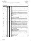
registers is as described in Table 1.
The contents of certain control registers are initialized to zero on
reset (see RESET pin description). Care should be exercised if the
contents of a register are changed during operation, since certain
changes may cause operational problems. For example, changing
the number of bits per character while the transmitter is active may
cause the transmission of an incorrect character. The contents of
the MR, the CSR, and the ACR should only be changed while the
receiver and transmitter are disabled, and certain changes to the
ACR should only be made while the C/T is stopped. The bit formats
of the UART are shown in Table 2.
MR1 – Mode Register 1
MR1 is accessed when the MR pointer points to MR1. The pointer is
set to MR1 by RESET or by a set pointer command applied via the
CR. After reading or writing MR1, the pointers are set at MR2.
MR1[7] – Receiver Request-to-Send Control
The bit controls the deactivation of the RTSN output (MPO) by the
receiver. This output is normally asserted and negated by
commands applied via the command register. MR1[7] = 1 causes
RTSN to be automatically negated upon receipt of a valid start bit if
the receiver FIFO is full. RTSN is reasserted when an empty FIFO
position is available. This feature can be used to prevent overrun in
the receiver by using the RTSN output signal to control the CTS
input of the transmitting device.
MR1[6] – Receiver Interrupt Select
This bit selects either the receiver ready status (RxRDY) or the FIFO
full status (FFULL) to be used for CPU interrupts.
MR1[5] – Error Mode Select
This bit selects the operating mode of the three FIFOed status bits
(FE, PE, received break). In the character mode, status is provided
on a character-by-character basis. The status applies only to the
character at the top of the FIFO. In the block mode, the status
provided in the SR for these bits is the accumulation (logical-OR) of
the status for all characters coming to the top of the FIFO since the
last reset error command was issued.
MR1[4:3] – Parity Mode Select
If with parity or force parity is selected, a parity bit is added to the
transmitted character and the receiver performs a parity check on
incoming data. MR![4:3] = 11 selects the channel to operate in the
special wake-up mode.
MR1[2] – Parity Type Select
This bit selects the parity type (odd or even) if the with parity mode
is programmed by MR1[4:3], and the polarity of the forced parity bit
if the force parity mode is programmed. It has no effect if the no


