


Philips Semiconductors Product data sheet
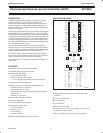
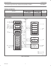
SCC2691Universal asynchronous receiver/transmitter (UART)
2006 Aug 04
6
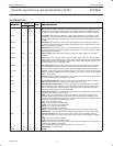
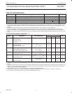
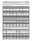
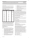
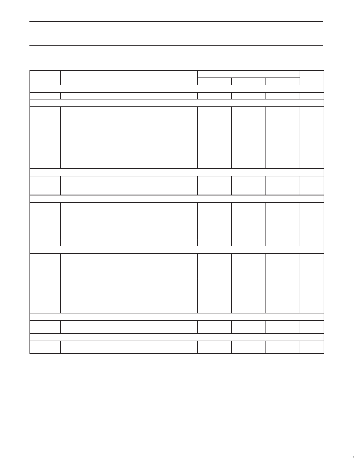
AC ELECTRICAL CHARACTERISTICS
1,
2,
3,
4
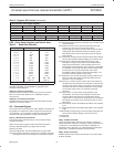
SYMBOL
PARAMETER
LIMITS
UNIT
SYMBOL
PARAMETER
Min Typ Max
UNIT
Reset timing (Figure 3)
t
RES
Reset pulse width 100 ns
Bus timing (Figure 4)
5
t
AS
A0–A2 setup time to RDN, WRN low 10 ns
t
AH
A0–A2 hold time from RDN, WRN low 100 ns
t
CS
CEN setup time to RDN, WRN low 0 ns
t
CH
CEN hold time from RDN, WRN high 0 ns
t
RW
WRN, RDN pulse width 150 ns
t
DD
Data valid after RDN low 125 ns
t
DF
Data bus floating after RDN high 110 ns
t
DS
Data setup time before WRN high 50 ns
t
DH
Data hold time after WRN high 30 ns
t
RWD
Time between reads and/or writes
6,
7
150 ns
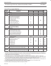
MPI and MPO timing (Figure 5)
5
t
PS
MPI input setup time before RDN low 30 ns
t
PH
MI input hold time after RDN low 30 ns
t
PD
MPO output valid after WRN high 370 ns
Interrupt timing (Figure 6)
t
IR
INTRN negated
Read RHR (RxRDY/FFULL interrupt) 370 ns
Write THR (TxRDY, TxEMT interrupt) 370 ns
Reset command (break change interrupt) 370 ns
Reset command (MPI change interrupt) 370 ns
Stop C/T command (counter interrupt) 370 ns
Write IMR (clear of interrupt mask bit) 270 ns
Clock timing (Figure 7)
t
CLK
X1/CLK high or low time 100 ns
f
CLK
9
X1/CLK frequency 0 4.0 MHz
t
CTC
Counter/timer clock high or low time 100 ns
f
CTC
8
Counter/timer clock frequency 0 4.0 MHz
t
RX
RxC high or low time 220 ns
f
RX
8
RxC frequency (16X)
RxC frequency (1X)
0
0
3.6864 2.0
1.0
MHz
MHz
t
TX
TxC high or low time 220 ns
f
TX
8
TxC frequency (16X)
TxC frequency (1X)
0
0
2.0
1.0
MHz
MHz
Transmitter timing (Figure 8)
t
TXD
TxD output delay from TxC external clock input on IP pin 350 ns
t
TCS
Output delay from TxC low at OP pin to TxD data output 0 150 ns
Receiver timing (Figure 9)
t
RXS
RxD data setup time before RxC high at external clock input on IP pin 100 ns
t
RXH
RxD data hold time after RxC high at external clock input on IP pin 100 ns
NOTES:
1. Parameters are valid over specified temp. range. See Ordering Information table for applicable operating temp. and V
CC
supply range.
2. All voltage measurements are referenced to ground (GND). For testing, all input signals swing between 0V and 3.0V with a transition time of
20ns max. For X1/CLK, this swing is between 0.4V and 4.0V. All time measurements are referenced at input voltages of 0.8V and 2V and
output voltages of 0.8V and 2V as appropriate.
3. Typical values are at +25°C, typical supply voltages, and typical processing parameters.
4. Test condition for outputs: C
L
= 150pF, except interrupt outputs. Test conditions for interrupt outputs: C
L
= 50pF, R
L
= 2.7kΩ to V
CC
.
5. Timing is illustrated and referenced to the WRN and RDN inputs. The device may also be operated with CEN as the ‘strobing’ input. In this
case, all timing specifications apply referenced to the falling and rising edges of CEN. CEN and RDN (also CEN and WRN) are ORed inter-
nally. As a consequence, this signal asserted last initiates the cycle and the signal negated first terminates the cycle.
6. If CEN is used as the ‘strobing’ input, this parameter defines the minimum high time between one CEN and the next. The RDN signal must
be negated for t
RWD
guarantee that any status register changes are valid.
7. Consecutive write operations to the command register require at least three rising edges of the X1 clock between writes.
8. These parameters are guaranteed by design, but are not 100% tested in production.
9. Operation to 0MHz is assured by design. Minimum test frequency is 2MHz.