


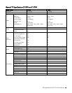
HP High-Definition LCD TV Service Manual 5
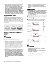
Attachment of SMDs
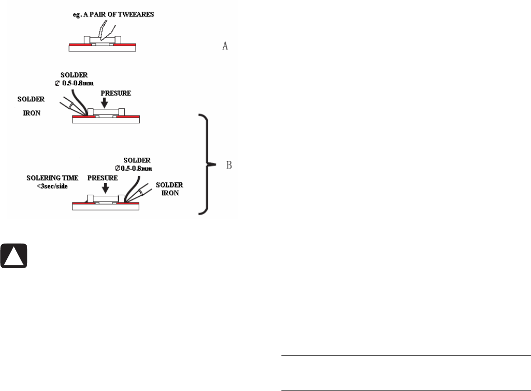
1 Locate the SMD on the solder lands by means of
tweezers and solder the component on one side.
Ensure that the component is positioned correctly on
the solder lands (A).
2 Complete the soldering of the terminals of the
component (B).
CAUTIONS:
• When soldering the SMD terminals, do not touch
them directly with the soldering iron. The soldering
should be done as quickly as possible; care must be
taken to avoid damage to the terminals of the SMDs
themselves.
• Keep the SMD’s body in contact with the printed
board when soldering.
• The soldering iron to be used (approximately 30 W)
should preferably be equipped with a thermal
control (soldering temperature: 360º to 380º C).
• Soldering should not be done outside the
solder land.
• Soldering flux (of rosin) may be used but should not
be acidic.
• After soldering, let the SMD cool down gradually at
room temperature.
• The quantity of solder must be proportional to the
size of the solder land. If the quantity is too great,
the SMD might crack or the solder lands might be
torn loose from the printed board.
Rework on Ball Grid Array (BGA) ICs
General information
Although (LF) BGA assembly yields are very high, there
may still be a requirement for component rework. By
rework
, we mean the process of removing the
component from the PWB and replacing it with a new
component. If an (LF) BGA is removed from a PWB, the
solder balls of the component are deformed drastically
so the removed (LF) BGA has to be discarded.
Device removal
As is the case with any component that, it is essential
when removing an (LF) BGA, the board, tracks, solder
lands, or surrounding components are not damaged.
To remove an (LF) BGA, the board must be uniformly
heated to a temperature close to the reflow soldering
temperature. A uniform temperature reduces the
chance of warping the PWB. To do this, we
recommend that the board is heated until it is certain
that all the joints are molten. Then carefully pull the
component off the board with a vacuum nozzle. For
the appropriate temperature profiles, see the IC data
sheet.
Area Preparation
When the component has been removed, the vacant IC
area must be cleaned before replacing the (LF) BGA.
Removing an IC often leaves varying amounts of solder
on the mounting lands. This excessive solder can be
removed with either a solder sucker or solder wick. The
remaining flux can be removed with a brush and
cleaning agent. After the board is properly cleaned
and inspected, apply flux on the solder lands and on
the connection balls of the (LF) BGA.
NOTE: Do not apply solder paste, as this has shown to
result in problems during resoldering.
Device replacement
The last step in the repair process is to solder the new
component on the board. Ideally, the (LF) BGA should
be aligned under a microscope or magnifying glass. If
this is not possible, try to align the (LF) BGA with any
board markers. To reflow the solder, apply a
temperature profile according to the IC data sheet. To
avoid damaging neighboring components, it may be
necessary to reduce some temperatures and times.