


HP High-Definition LCD TV Service Manual 3
• Be sure to handle the circuit board by holding the
large parts such as the heat sink or transformer.
Failure to observe this precaution may result in the
occurrence of an abnormality in the soldered areas.
• Do not stack the circuit boards. Failure to observe
this precaution may result in problems resulting from
scratches on the parts, the deformation of parts, and
short-circuits due to residual electric charge.
• Routing the wires and fixing them in position must
be done in accordance with the original routing and
fixing configuration when servicing is completed. All
the wires are routed far away from the areas that
become hot (such as the heat sink). These wires are
fixed in position with the wire clamps so that the
wires do not move, thereby ensuring that they are
not damaged and their materials do not deteriorate
over long periods of time. Therefore, route the
cables and fix the cables to the original position
and states using the wire clamps.
• Perform a safety check when servicing is completed.
Verify that the peripherals of the serviced points
have not undergone any deterioration during
servicing. Also verify that the screws, parts, and
cables removed for servicing purposes have all
been returned to their proper locations in
accordance with the original setup.
• A glass plate protects the LCD display. This glass
plate can be cleaned with a slightly moist cloth. If
dirt appears between the glass plate and the LCD
display panel have only a qualified service
employee clean it.
Repair Tips
WARNING: All ICs and many other
semiconductors are susceptible to electrostatic
discharges (ESDs). Careless handling during repair
can be life-threatening. When repairing, make sure
that you are connected with the same potential as
the mass of the unit via a wrist wrap with
resistance. Keep components and tools also at the
same potential.
About Lead-Free Solder
NOTE: LEAD IS LISTED AS (PB) IN THE PERIODIC
TABLE OF THE ELEMENTS. IN THE INFORMATION
THAT FOLLOWS, PB WILL REFER TO LEAD SOLDER,
AND PBF WILL REFER TO LEAD-FREE SOLDER. THE
LEAD-FREE SOLDER USED IN OUR MANUFACTURING
PROCESS AND DISCUSSED HERE IS (SN+AG+CU).
THAT IS TIN (SN), SILVER (AG), AND COPPER (CU),
ALTHOUGH OTHER TYPES ARE AVAILABLE.
This model is manufactured using Pb-free solder for the
sake of environmental conservation. For service and
repair work, we suggest using Pb-free solder as well,
although Pb solder may be used.
PCBs manufactured using Pb-free solder have the sign
stamped on the PCB.
CAUTIONS:
• Pb-free solder has a higher melting point than Pb
solder. Typically the melting point is 50–70ºF
(30–40°C) higher. Use a high temperature soldering
iron. Adjust your solder tool so that a temperature
around 360–380ºC is reached and stabilized at the
solder joint. Heating time of the solder joint should
not exceed 4 seconds. Avoid temperatures above
400ºC; wear-out of tips will rise drastically and flux-
fluid will be destroyed.
• Pb-free solder will tend to splash when heated too
high (about 1,100ºF or 600ºC).
• Mix of Pb-free solder Tin (SN)/parts with leaded
soldering Tin (SN) in/parts is possible but not
recommended. If you have to use Pb solder,
completely remove all of the Pb-free solder on the
pins or solder area before applying Pb solder. If this
is not practical, be sure to heat the Pb-free solder
until it melts, before applying Pb solder.
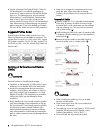
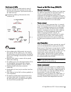
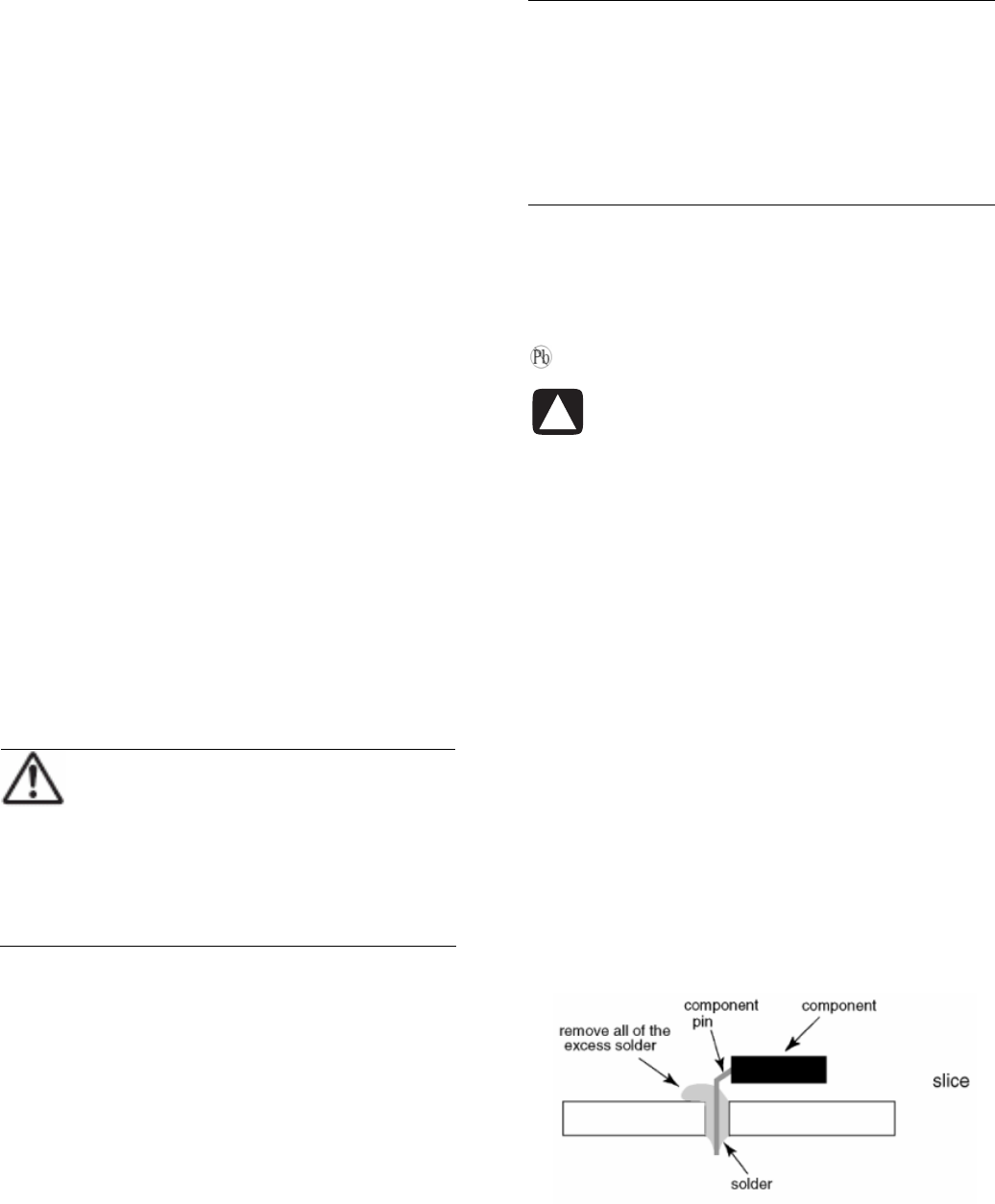
• After applying Pb-free solder to double-layered
boards, check the component side for excess solder
that may flow onto the opposite side (see the
following illustration).