


1. Product Specification (continued)
1.3.2 Video Input Signals
1.3.2.1 Video Signal Amplitudes
The three video inputs consist of Red ,Green , and Blue
signals, each with its own coaxial cable terminated at the
monitor. These video signals are analog levels, where 0
V corresponds to black , and 700 mV is the maximum
signal amplitude for the respective color, when each
signal is terminated by a nominal 75.0 ohms .For a given
monitor luminance levels are measured using this
defined video amplitud driving a monitor meeting the
termination requirements .The signal amplitude is not to
be readjusted to compensate for variations in termination
impedance.
1.3.2.2 Video Signal Termination Impedance
This analog video signal termination shall be 75 1%
which shall be resistive with a negligible reactive
component
1.3.2.3 Synchronization ( Sync ) Signals
The Horizontal Sync (HS) TTL signal is used to initiate
the display of a horizontal line. HS may be either active
high or active low, depending upon the timing .The
Vertical Sync (VS) TTL signal is used to initiate the
display of a new frame .VS may be either active high or
active low, depending on the timing
1.3.2.4 Sync Signal Levels
The monitor must accept sync signals from both 3.3 and
5 volt TTL logic families.The inputs shall sense a logic 0
when the input is 0.8 volt or less and shall sense a logic
1 when the input is 2.0 volts or greater. In addition to
these level requirements, there shall also be a minimum
of 0.3 volt hysteresis provided for noise immunity
(typically by using a Schmitt Trigger input ).That is , the
input level at which the monitor actually detects a logic 0
shall be at least 0.3 volt lower than the level at which it
actually detects a logic 1.If the monitor sync processing
circuits are designed around the 3.3 volt logic family
,then the sync inputs must be 5 volt tolerant .
TTL input loading shall be equivalent to one TTL input
load. When logic 0 is asserted by a sync input , the
maximum current source from any single monitor sync
input to the driver is 1.6 mA .When logic 1 is asserted ,
the maximum current source from the driver to any
single monitor sync input is 400 uA .
Ω+/-
.
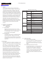
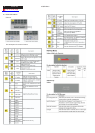
1.3.2.5 Sync Signal Loading
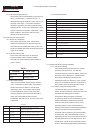
DSUB
P in S ig n a l P in S ig n a l P in S ig n a l
1
Red-Video
6
Red-GND
11
NC
2
Green-Video
7
Green-GND
12
DDC-SDA
3
Blue-Video
8
Blue-GND
13
H-SYNC
4
NC
9
+5V
14
V-SYNC
5
DDC-GND
10
Sync-GND
15
DDC-SCL
Connector Pin Assignment
D-SUB PinDescription
Pin N ame D e scription
1 Red-Video Red video signal input.
2 Green-Video Green video signalinput.
3 Blue-Video Blue video signal input.
4GND Ground
5 DDC-GN D DDC ground for the VESA DDC2Bi function.
6 Red- GND Ana lo g s igna lgro und fo r the Re d vide o.
7 Green-GN D Analog signalground for the Greenvideo.
8 Blue- GND A na lo g signal gro und for the B lue vid e o .
9 + 5V + 5V input from ho stsystem for the VES A DD C 2 Bifunction.
10 Sync-GND Signalground
11 GN D Ground
12 DDC_SDA SDA signal inputfor the VESA DDCB2i function.
13 H -S Y NC H orizontalsignalinp ut fro m the host system.
14 V -S Y NC V erticalsignalinput from the ho stsystem.
15 DDC-SC L SCL signal inputfor the VESA DDC 2Bi function.
Connector Pin Description
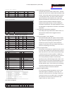
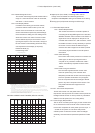
DVI- I / DVI-D (If using D VI-D cable, C1, C2, C3, C4, C5 is NC)
Pin Signal Pin Signa l Pin Signa l
1
RX2-
11
GND
21
NC
2
RX2+
12
NC
22
GND
3
GND
13
NC
23
RXC+
4
NC
14
5V
24
RXC-
5
NC
15
GND
C1
Analog Red (NC)
6
SCL
16
HP
C2
Analog Green (NC)
7
SCA
17
RX0-
C3
Analog Blue (NC)
8
Analog V-Sync (NC)
18
RX0+
C4
Analog H-Sy nc (NC)
9
RX1-
19
GND
C5
GND
10
RX1+
20
NC
DV I-I /DV I-DCon nectorPinDescrip tion
P in Name Descr ip tion P in Name Descr ip tion
1 R X 2- T M D Sli n k#0chan n el#2 di f f eren tialpai r 1 6 H P H otpl u gg i n g
2 R X 2+ T M D Sl i n k#0chan n el#2 di f f eren tialpair 17 RX 0- T M D Sli n k#0chan n el#0dif fere nti alpair
3 GND GNDfor nolink share 18 RX0+ TMDS link #0 channel#0 differentialpair
4 NC NC 19 GND GNDfor nolink share
5NC NC 20NC NC
6 SCL Clockl in eforDD Cin terface 21 NC NC
7 SDA Datalinefor DDC interface 22 GND Clockshield
8
Analog
V-Sync
V-syncfor analoginterface 23 RXC+ TMDS clockdifferential pair
9 RX1- TMDS link#0channel#1 differentialpair 24 RXC- TMDS clock differentialpair
10 RX 1+ TMDSli nk#0ch an n el#1di ff eren tialpair C1
Analog
Red
Analog Red signal
11 G ND GNDfornol in kshare C2
Analog
Green
Analog Green signal
12 NC NC C3
Analog
Blue
Analog Blue signal
13 NC NC C4
Analog
H-Sync
H-sync foranaloginterface
14 5V +5Vi npu tfromh ostsy stemf orDD C2Bfu ncti on. C5
Analog
GND
Analog GND
15 GND G rou n d(U si n gasDetectCabl e)
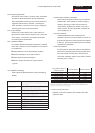
No. Symbol Item Min
Normal
Max Unit Remark
1
Fh Scanning Horizontal Frequency 30 94 kHz M inimum range
2
Fv Scanning Vertical Frequency 55 76 Hz M inimum range
3
Vih HiLevelInput 2 5 Note 1)
4
Vil Low Level Input 0 0.8 V Note1)
5
Video RGB Analog Video Level 0.0 0.7 1.0 V
75
Ω
to Ground
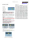
N ote 1) Schm itt-T rig gers In pu t , S upported 3.3V device H(&V) sync outputfrom PC.
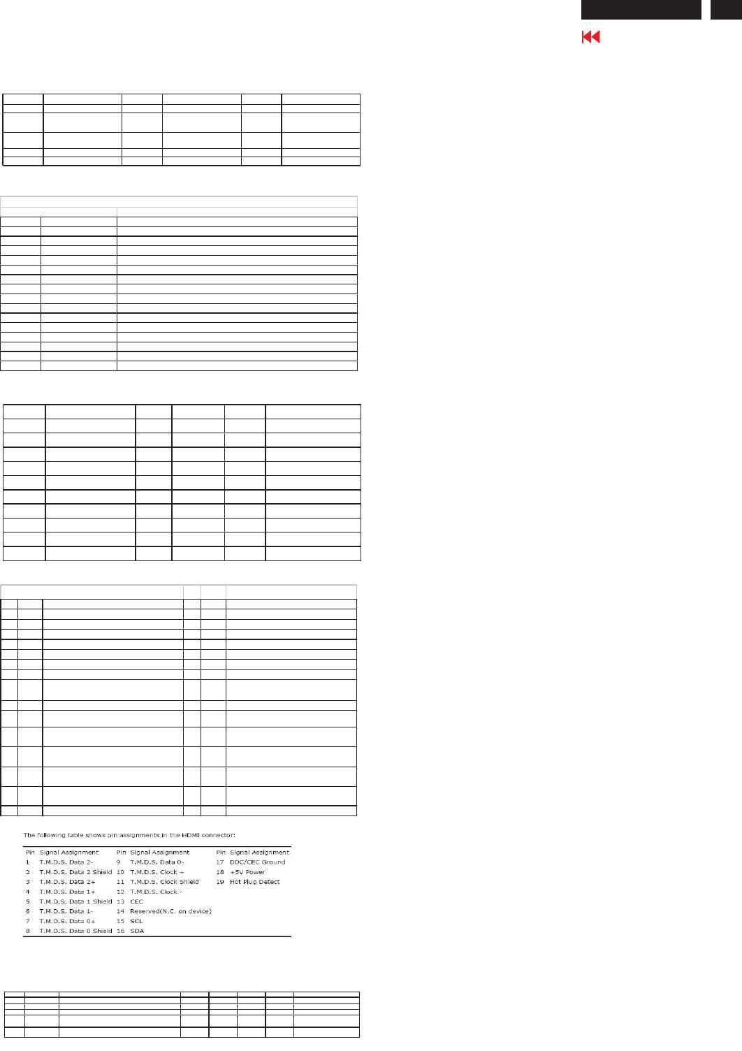
Video Input Signal
Go to cover page
3
ACER G24