


3 - 14 3 - 14
MELSEC-Q
3 SPECIFICATIONS
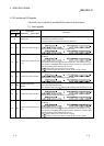
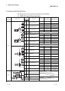
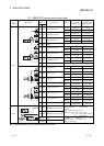
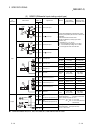
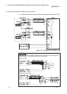
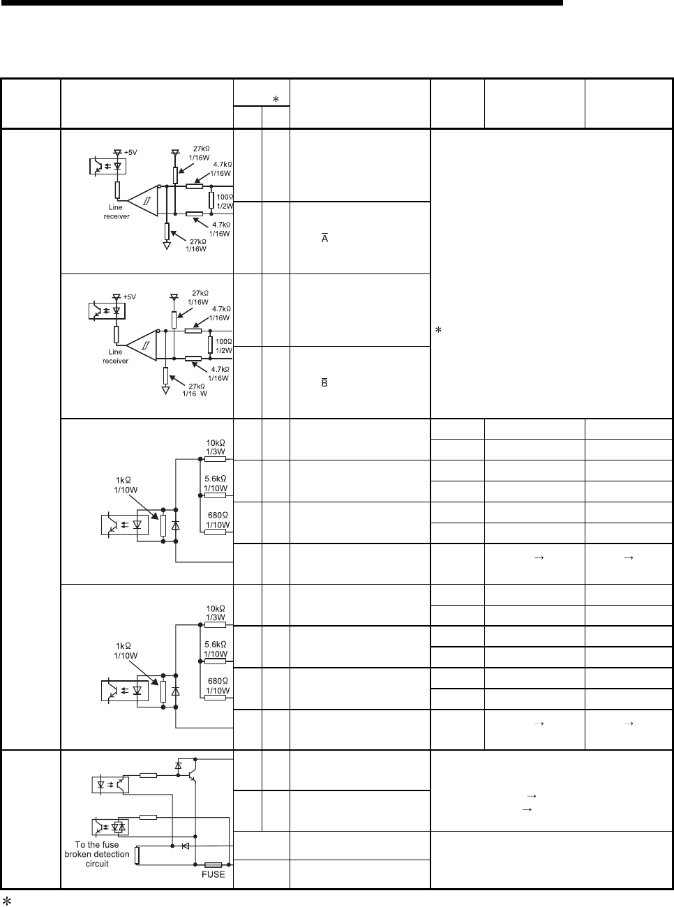
(3) QD62D (Differential input sinking output type)
Terminal
number
1
I/O
classification
Internal circuit
CH1 CH2
Signal name
Operation
Input voltage
(guaranteed value)
Operating current
(guaranteed value)
A20 A14 Phase A pulse input
B20 B14 Phase pulse input
A19 A13 Phase B pulse input
A19 B13 Phase
pulse input
Line driver level (AM26LS31 [manufactured by Texas
Instruments] or equivalent) that conforms to RS-422-A in
EIA Standard
EIA standard RS-422-A line driver level
Equivalent to AM26LS31 (made by Japan Texas
Instruments, Inc.)
V
hys Hysteresis (VT+ - VT-) 60 mV
V
IH(E) "H" level enable input voltage: 2 V or higher
V
IL(E) "L" level enable input voltage: 0.8 V or lower
A current type line driver cannot be used.
When ON 21.6 to 26.4 V 2 to 5 mA
A18 A12 Preset input 24 V
When OFF 5 V or less 0.1 mA or less
When ON 10.8 to 13.2 V 2 to 5 mA
B18 B12 Preset input 12 V
When OFF 4 V or less 0.1 mA or less
When ON 2.5 to 5.5 V 2 to 5 mA
A17 A11 Preset input 5 V
When OFF 1 V or less 0.1 mA or less
B17 B11 PRSTCOM
Response
time
OFF
ON
0.5 ms or less
ON OFF
1 ms or less
When ON 21.6 to 26.4 V 2 to 5 mA
A16 A10 Function start input 24 V
When OFF 5 V or less 0.1 mA or less
When ON 10.8 to 13.2 V 2 to 5 mA
B16 B10 Function start input 12 V
When OFF 4 V or less 0.1 mA or less
When ON 2.5 to 5.5 V 2 to 5 mA
A15 A09 Function start input 5 V
When OFF 1 V or less 0.1 mA or less
Input
B15 B09 FUNCCOM
Response
time
OFF
ON
0.5 ms or less
ON OFF
1 ms or less
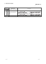
A06 A05
EQU1
(Coincidence output point No. 1)
B06 B05
EQU2
(Coincidence output point No. 2)
Operating voltage 10.2 to 30 V
Maximum load current 0.5 A/point, 2 A/common
Maximum voltage drop when ON 1.5 V
Response time OFF
ON 0.1 ms or less
ON
OFF 0.1 ms or less (rated load,
resistive load)
B02, B01 12/24 V
Output
A02, A01 0 V
Input voltage 10.2 to 30 V
Current consumption 8 mA (TYP 24 V DC)
Common for all channels
1: Terminal numbers A08, A07, A03, A04, B08, B07, B04 and B03 are not used.