


CONFIDENTIAL – DO NOT COPY
Page 7-15
File No. SG-0198
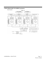
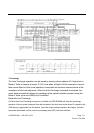
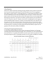
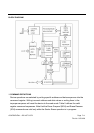
5. Read Operation
With the DLL enabled, all devices operating at the same frequency within a system are ensured to
have the same timing relationship between DQ and DQS relative to the CK input regardless of
device density, process variation, or technology generation. The data strobe signal (DQS) is driven
off chip simultaneously with the output data (DQ) during each read cycle. The same internal clock
phase is used to drive both the output data and data strobe signal off chip to minimize skew between
data strobe and output data. This internal clock phase is nominally aligned to the input differential
clock (CK, CK) by the on-chip DLL. Therefore, when the DLL is enabled and the clock frequency is
within the specified range for proper DLL operation, the data strobe (DQS), output data (DQ), and
the system clock (CK) are all nominally aligned. Since the data strobe and output data are tightly
coupled in the system, the data strobe signal may be delayed and used to latch the output data into
the receiving device. The tolerance for skew between DQS and DQ (tDQSQ) is tighter than that
possible for CK to DQ (tAC) or DQS to CK (tDQSCK).
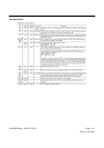
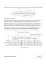
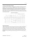
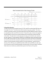
6. Precharge Timing During Read Operation
For the earliest possible Precharge command without interrupting a Read burst, the Precharge
command may be issued on the rising clock edge, which is CAS latency (CL) clock cycles before the
end of the Read burst. A new Bank Activate (BA) command may be issued to the same bank after
the RAS precharge time (tRP). A Precharge command can not be issued until tRAS(min) is satisfied.