


CONFIDENTIAL – DO NOT COPY
Page 7-41
File No. SG-0198
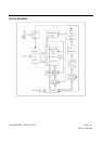
STANDBY MODE
MX29LV320AT/B can be set into Standby mode with two different approaches. One is using both CE
and RESET pins and the other one is using RESET pin only.
When using both pins of CE and RESET, a CMOS Standby mode is achieved with both pins held at
Vcc ±0.3V. Under this condition, the current consumed is less than 0.2uA (typ.). If both of the CE and
RESET are held at VIH, but not within the range of VCC ± 0.3V, the device will still be in the standby
mode, but the standby current will be larger. During Auto Algorithm operation, Vcc active current
(ICC2) is required even CE = "H" until the operation is completed. The device can be read with
standard access time (tCE) from either of these standby modes.
When using only RESET, a CMOS standby mode is achieved with RESET input held at Vss ± 0.3V,
Under this condition the current is consumed less than 1uA (typ.). Once the RESET pin is taken high,
the device is back to active without recovery delay.In the standby mode the outputs are in the high
impedance state, independent of the OE input.MX29LV320AT/B is capable to provide the Automatic
Standby Mode to restrain power consumption during readout of data. This mode can be used
effectively with an application requested low power consumption such as handy terminals.
To active this mode, MX29LV320AT/B automatically switch themselves to low power mode when
MX29LV320AT/B addresses remain stable during access time of tACC+30ns. It is not necessary to
control CE, WE, and OE on the mode. Under the mode, the current consumed is typically 0.2uA
(CMOS level).
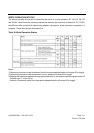
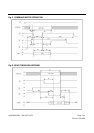
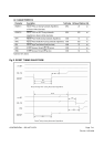
RESET OPERATION
01The RESET pin provides a hardware method of resetting the device to reading array data. When
the RESET pin is driven low for at least a period of tRP, the device immediately terminates any
operation in progress, tristates all output pins, and ignores all read/write commands for the duration
of the RESET pulse. The device also resets the internal state machine to reading array data. The
operation that was interrupted should be reinitiated once the device is ready to accept another
command sequence, to ensure data integrity.
Current is reduced for the duration of the RESET pulse. When RESET is held at VSS 0.3V, the
device draws CMOS standby current (ICC4). If RESET is held at VIL but not within VSS 0.3V, the
standby current will be greater.The RESET pin may be tied to system reset circuitry. A system reset
would that also reset the Flash memory, enabling the system to read the boot-up firm-ware from the
Flash memory.