


CONFIDENTIAL – DO NOT COPY
Page 7-17
File No. SG-0198
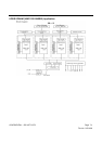
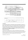
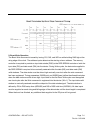
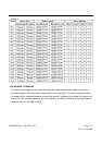
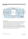
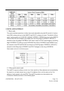
9. Burst Write Operation
The Burst Write command is issued by having CS, CAS, and WE low while holding RAS high at the
rising edge of the clock. The address inputs determine the starting column address. The memory
controller is required to provide an input data strobe (DQS) to the DDR SDRAM to strobe or latch the
input data (DQ) and data mask (DM) into the device. During Write cycles, the data strobe applied to
the DDR SDRAM is required to be nominally centered within the data (DQ) and data mask (DM)
valid windows. The data strobe must be driven high nominally one clock after the write command
has been registered. Timing parameters tDQSS(min) and tDQSS(max) define the allowable window
when the data strobe must be driven high. Input data for the first Burst Write cycle must be applied
one clock cycle after the Write command is registered into the device (WL=1). The input data valid
window is nominally centered around the midpoint of the data strobe signal. The data window is
defined by DQ to DQS setup time (tQDQSS) and DQ to DQS hold time (tQDQSH). All data inputs
must be supplied on each rising and falling edge of the data strobe until the burst length is completed.
When the burst has finished, any additional data supplied to the DQ pins will be ignored.