


CONFIDENTIAL – DO NOT COPY
Page 7-20
File No. SG-0198
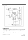
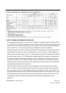
2. WRITE COMMANDS/COMMAND SEQUENCES
To program data to the device or erase sectors of memory, the system must drive WE and CE to
VIL, and OE to VIH. The device features an Unlock Bypass mode to facilitate faster programming.
Once the device enters the Unlock Bypass mode, only two write cycles are required to program a
byte, instead of four. The "byte Program Command Sequence" section has details on
programming data to the device using both standard and Unlock Bypass command sequences. An
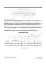
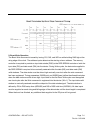
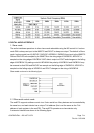
erase operation can erase one sector, multiple sectors, or the entire device. Table indicates the
address space that each sector occupies. A "sector address" consists of the address bits required
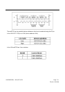
to uniquely select a sector. The "Writing specific address and data commands or sequences into
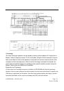
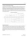
the command register initiates device operations. Figure 1 defines the valid register command
sequences. Writing incorrect address and data values or writing them in the improper sequence
resets the device to reading array data. Section has details on erasing a sector or the entire chip,
or suspending/resuming the erase operation.
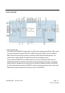
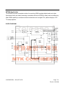
After the system writes the auto select command sequence, the device enters the auto select
mode. The system can then read auto select codes from the internal register (which is separate
from the memory array) on Q7-Q0. Standard read cycle timings apply in this mode. Refer to the
Auto select Mode and Auto select Command Sequence section for more information. ICC2 in the
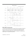
DC Characteristics table represents the active current specification for the write mode. The "AC
Characteristics" section contains timing specification table and timing diagrams for write
operations.