


CONFIDENTIAL – DO NOT COPY
Page 7-46
File No. SG-0198
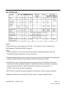
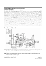
DDR SDRAM (NT5DS16M16CS-5T) Application:
Functional Description
The 256Mb DDR SDRAM is a high-speed CMOS, dynamic random-access memory containing 268,
435, 456 bits. The 256Mb DDR SDRAM is internally configured as a quad-bank DRAM. The 256Mb
DDR SDRAM uses a double-data-rate architecture to achieve high-speed operation. The
double-data-rate architecture is essentially a 2n prefetch architecture, with an interface designed to
transfer two data words per clock cycle at the I/O pins. A single read or write access for the 256Mb
DDR SDRAM consists of a single 2n-bit wide, one clock cycle data transfer at the internal DRAM
core and two corresponding n-bit wide, one-half clock cycle data transfers at the I/O pins. Read and
write accesses to the DDR SDRAM are burst oriented; accesses start at a selected location and
continue for a programmed number of locations in a programmed sequence. Accesses begin with
the registration of an Active command, which is then followed by a Read or Write command. The
address bits registered coincident with the Active command are used to select the bank and row to
be accessed (BA0, BA1 select the bank; A0-A12 select the row). The address bits registered
coincident with the Read or Write command are used to select the starting column location for the
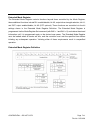
burst access.Prior to normal operation, the DDR SDRAM must be initialized. The following sections
provide detailed information covering device initialization, register definition, command descriptions
and device operation.
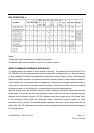
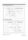
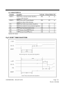
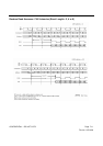
Block Diagram (16Mb x 16)
Note: This Functional Block Diagram is intended to facilitate user understanding of the operation of
the device; it does not represent an actual circuit implementation.
Note: DM is a unidirectional signal (input only), but is internally loaded to match the load of the
bidirectional DQ and DQS signals.