


Page 37
MODELS: WD-60C9 / WD-65C9 / WD-73C9 / WD-60737 / WD-65737 / WD-73737 / WD-82737
WD-65837 / WD-73837 / WD-82837
Using Lead Free Solder
Pb Solder
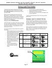
The symbol shown below indicates Lead (Pb) Free
solder was used during the construction of PWBs.
Only Lead Free solder should be used when servic-
ing these PWBs.
Solder must be compatible with that used by the
manufacturer. Leaded solder can not be used on
PWBs manufactured with Pb-free solder. The Mitsub-
ishi standard for service requires the use of Tin-Silver-
Copper (Sn-96.5, Ag-3.0, Cu-0.5). It can be obtained
through the Parts Department.
Order part number: PB FREE SOLDER
Lead Free solder has a higher melting point, and does
not “wet” as well as leaded solder. This means it does
not adhere as readily to the solder iron tip, and the
surface to be soldered. To counteract this, the flux
used is more corrosive.
The following cautions must be taken when using Pb
Free solder.
• Higher temperatures can cause the PWB to
warp, detaching surface mount components.
• Higher temperatures may cause
thermal damage to components.
• Higher temperatures can cause
plastics, such as connectors,
relays, LEDs electrolytic
capacitors, etc. to melt or warp.
• Higher temperatures can cause
surface oxidation resulting in
poor solder spread-ability and
wet-ability.
• The flux is more corrosive.
• The time required for a good
solder connection may take
longer.
• Poor wet-ability can cause solder balls.
• Higher temperatures can cause flux spattering.
• Soldering iron tip life is shortened.
• Dull finish solder joints (not shiny) can appear to be
a “cold” solder joint.
In general a tip temperature of 700° F will usually provide
good results.
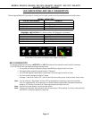
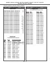
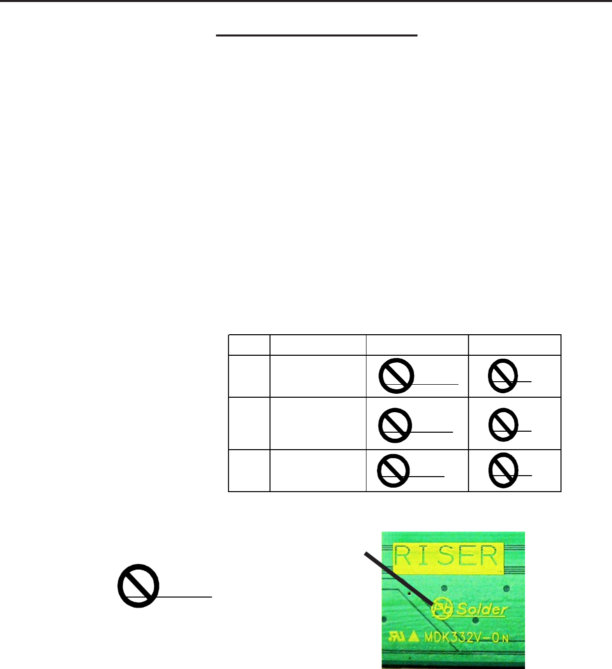
Displays used to indicate Pb-free
PCBs will be marked, indicating the level of Pb-free con-
struction. Table 1 defines the levels by phase and shows
the different symbols that will be displayed on the PCB.
Additionally, a PCB constructed using Pb-free solder may
be simply marked LFS.
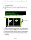
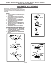
When possible, the indication will be placed close to the
part number that is screened onto the PCB (not the part
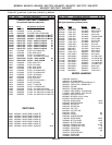
label). Figure 1 is an example of a PCB showing the
display and its location.
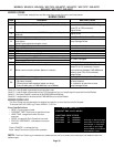
Pb-Free
Phase Definition Display
Short Displa
y
(
When the
area is too small)
Phase-1 PCB's constructed using
Pb-free solder.
Phase-2 Solder, PCB surface
finishing and component
lead plating is Pb-free.
Components may have
internal Pb.
Phase-3 Solder, PCB surface
finishin
g
and components
are Pb-free. (100% Pb-
free)
Table 1: Pb-Free Phases and Symbols
Pb PCA
Pb Joints
Pb S
Pb J
Pb P
Pb Solder
Pb-Free
Display
Figure 1: Pb-Free display on PWB