Introduction
6
SLES140A—March 2007TVP5147M1PFP
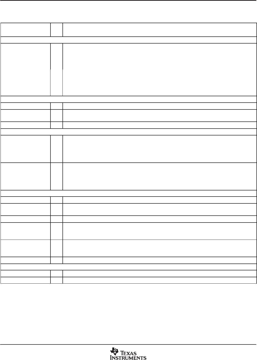
1.7 Terminal Functions
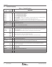
Table 1−1. Terminal Functions
TERMINAL
I/O
DESCRIPTION
NAME NUMBER
I/O
DESCRIPTION
Analog Video
VI_1_A
VI_1_B
VI_1_C
VI_2_A
VI_2_B
80
1
2
7
8
I/O
I
I
I
I
VI_1_A: Analog video input for CVBS/Pb/C or analog video output (see Section 2.11.59)
VI_1_x: Analog video input for CVBS/Pb/C
VI_2_x: Analog video input for CVBS/Y
VI_3_x: Analog video input for CVBS/Pr/C
VI_4_A: Analog video input for CVBS/Y
VI_2_B
VI_2_C
VI_3_A
VI_3_B
VI_3_C
VI_4_A
8
9
16
17
18
23
I
I
I
I
I
I
VI_4_A: Analog video input for CVBS/Y
Up to 10 composite, 4 S-video, and 2 composite or 3 component video inputs (or a combination thereof)
can be supported.
The inputs must be ac-coupled. The recommended coupling capacitor is 0.1 µF.
The possible input configurations are listed in the input select register at I
2
C subaddress 00h (see
Section 2.11.1).
Clock Signals
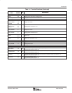
DATACLK 40 O Line-locked data output clock
XTAL1 74 I
External clock reference input. It can be connected to an external oscillator with a 1.8-V compatible clock
signal or a 14.31818-MHz crystal oscillator.
XTAL2 75 O External clock reference output. Not connected if XTAL1 is driven by an external single-ended oscillator.
Digital Video
C_[9:0]/
GPIO[9:0]
57, 58,
59, 60,
63, 64,
65, 66,
69, 70
I/O
Digital video output of CbCr, C[9] is MSB and C[0] is LSB. Also, these terminals can be programmable
general-purpose I/O.
For the 8-bit mode, the two LSBs are ignored. Unused outputs can be left unconnected.
Y[9:0]
43, 44,
45, 46,
47, 50,
51, 52,
53, 54
O
Digital video output of Y/YCbCr, Y[9] is MSB and Y[0] is LSB.
For the 8-bit mode, the two LSBs are ignored. Unused outputs can be left unconnected.
Miscellaneous Signals
GPIO 35 I/O Programmable general-purpose I/O
GLCO/I2CA 37 I/O
Genlock control output (GLCO) uses real time control (RTC) format.
During reset, this terminal is an input used to program the I
2
C address LSB.
INTREQ 30 O Interrupt request
NC
14, 15,
19, 20,
21, 22
Not connected. These terminals can be connected to power or ground (compatible with TVP5146
terminals), internally floating.
PWDN 33 I
Power down input:
1 = Power down
0 = Normal mode
RESETB 34 I Reset input, active low (see Section 2.8)
Host Interface
SCL 28 I I
2
C clock input
SDA 29 I/O I
2
C data bus


