


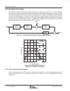
Functional Description
22
SLES140A—March 2007TVP5147M1PFP
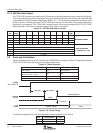
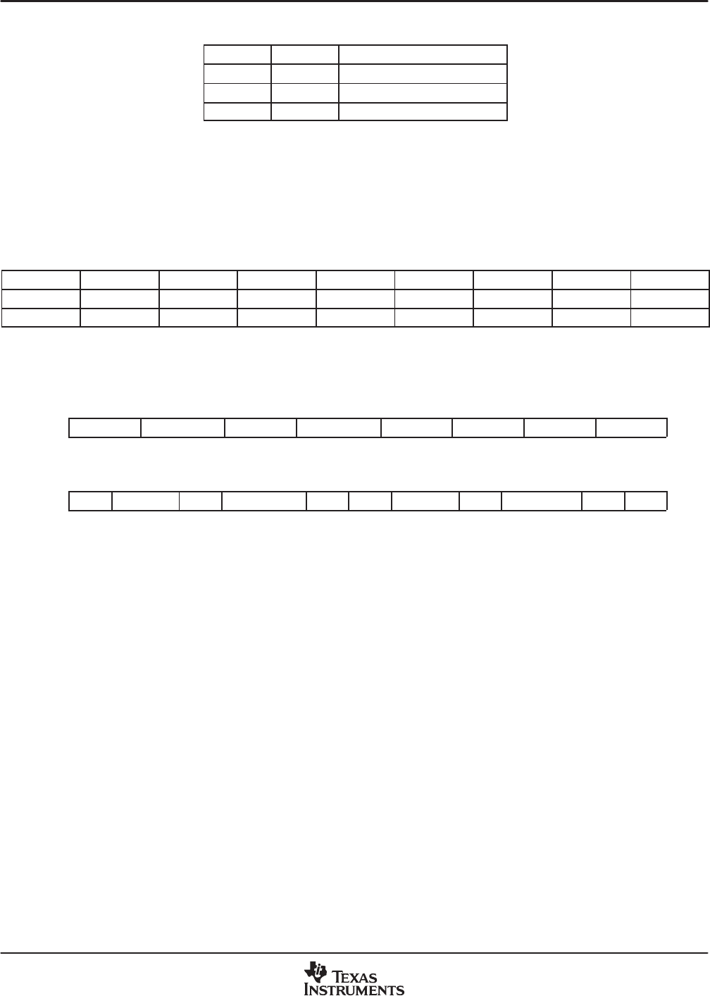
Table 2−4. I
2
C Host Interface Terminal Description
SIGNAL TYPE DESCRIPTION
I2CA I Slave address selection
SCL I Input clock line
SDA I/O Input/output data line
2.6.1 Reset and I
2
C Bus Address Selection
The TVP5147M1 decoder can respond to two possible chip addresses. The address selection is made at reset
by an externally supplied level on the I2CA terminal. The TVP5147M1 decoder samples the level of terminal
37 at power up or at the trailing edge of RESETB and configures the I
2
C bus address bit A0. The I2CA terminal
has an internal pulldown resistor to pull the terminal low to set a zero.
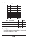
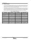
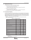
Table 2−5. I
2
C Address Selection
A6 A5 A4 A3 A2 A1 A0 (I2CA) R/W HEX
1 0 1 1 1 0 0 (default) 1/0 B9/B8
1 0 1 1 1 0 1
†
1/0 BB/BA
†
If terminal 37 is strapped to DVDD via a 2.2-kΩ resistor, I
2
C device address A0 is set to 1.
2.6.2 I
2
C Operation
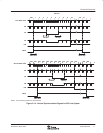
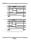
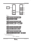
Data transfers occur using the following illustrated formats.
S 10111000 ACK Subaddress ACK Send data ACK P
Read from I
2
C control registers
S 10111000 ACK Subaddress ACK S 10111001 ACK Receive data NAK P
S = I
2
C bus start condition
P = I
2
C bus stop condition
ACK = Acknowledge generated by the slave
NAK = Acknowledge generated by the master, for multiple-byte read master with ACK each byte except
last byte
Subaddress = Subaddress byte
Data = Data byte. If more than one byte of data is transmitted (read and write), the subaddress pointer is
automatically incremented.
I
2
C bus address = Example shown that I
2
CA is in default mode. Write (B8h), read (B9h)
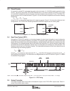
2.6.3 VBUS Access
The TVP5147M1 decoder has additional internal registers accessible through an indirect access to an internal
24-bit address wide VBUS. Figure 2−17 shows the VBUS register access.