


TDA8752B
Triple high-speed Analog-to-Digital Converter 110 Msps
Rev. 03 — 21 July 2000 Product specification
c
c
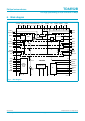
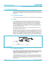
1. General description
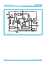
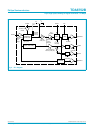
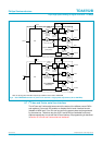
The TDA8752B is a triple 8-bit ADC with controllable amplifiers and clamps for the
digitizing of large bandwidth RGB signals.
The clamp level, the gain and all other settings are controlled via a serial interface
(either I
2
C-bus or 3-wire serial bus, selected via a logic input).
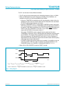
The IC also includes a PLL that can be locked to the horizontal line frequency and
generates the ADC clock. The PLL jitter is minimized for high resolution PC graphics
applications. An external clock can also be input to the ADC.
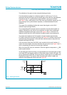
It is possible to set the TDA8752B serial bus address to four different values, when
several TDA8752B ICs are used in a system, by means of the I
2
C-bus interface (for
example, two ICs used in an odd/even configuration).
2. Features
■ Triple 8-bit ADC
■ Sampling rate up to 110 Msps
■ IC controllable via a serial interface, which can be either I
2
C-bus or 3-wire serial
bus, selected via a TTL input pin
■ IC analog voltage input from 0.4 to 1.2 V (p-p) to produce a full-scale ADC input of
1 V (p-p)
■ Three clamps for programming a clamping code between −63.5 and +64 in steps
of
1
⁄
2
LSB for RGB signals, and from +120 to +136 in steps of
1
⁄
2
LSB for YUV
signals
■ Three controllable amplifiers: gain controlled via the serial interface to produce a
full-scale resolution of
1
⁄
2
LSB peak-to-peak
■ Amplifier bandwidth of 250 MHz
■ Low gain variation with temperature
■ PLL controllable via the serial interface to generate the ADC clock which can be
locked to a line frequency of 15 to 280 kHz
■ Integrated PLL divider
■ Programmable phase clock adjustment cells
■ Internal voltage regulators
■ TTL compatible digital inputs and outputs
■ Chip enable high-impedance ADC output