


Philips Semiconductors
TDA8752B
Triple high-speed Analog-to-Digital Converter 110 Msps
Product specification Rev. 03 — 21 July 2000 22 of 38
9397 750 07338
© Philips Electronics N.V. 2000. All rights reserved.
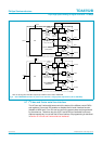
9.2 I
2
C-bus protocol
The I
2
C-bus address of the circuit is 1001 1xx0.
Bits ‘A2’ and ‘A1’ are fixed by the potential on pins ADD1 and ADD2. Thus, four
TDA8752Bs can be used on the same system, using the addresses for
ADD1 and ADD2 with the I
2
C-bus. Bit ‘A0’ must always be equal to logic 0 because it
is not possible to read the data in the register. The timing and protocol for the I
2
C-bus
are standard. Two sequences are available, see Tabl e 13 and 14.
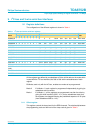
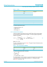
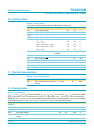
Table 12: I
2
C-bus address
A7 A6 A5 A4 A3 A2 A1 A0
1 0 0 1 1 ADD2 ADD1 0
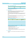
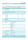
Table 13: Address sequence for mode 0
Where: S = START condition, ACK = acknowledge and P = STOP condition.
S IC ADDRESS ACK SUBADDRESS
REGISTER1
ACK DATA
REGISTER1
(see Tabl e 4)
ACK SUBADDRESS
REGISTER2
ACK ... P
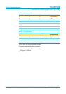
Table 14: Address sequence for mode 1
Where: S = START condition, ACK = acknowledge and P = STOP condition.
S IC ADDRESS ACK SUBADDRESS
XXX1 1111
ACK DATA
REGISTER1
(see Tabl e 4)
ACK DATA
REGISTER2
ACK ... P