


Philips Semiconductors
TDA8752B
Triple high-speed Analog-to-Digital Converter 110 Msps
Product specification Rev. 03 — 21 July 2000 28 of 38
9397 750 07338
© Philips Electronics N.V. 2000. All rights reserved.
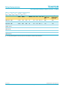
ADC data outputs
V
OL
LOW-level output voltage I
o
=1mA − 0 0.4 V
V
OH
HIGH-level output voltage I
o
= −1 mA 2.4 V
CCD
− V
I
OL
LOW-level output current V
OL
= 0.4 V − 2 − mA
I
OH
HIGH-level output current V
OH
= 2.7 V −−0.4 − mA
TTL digital inputs (CKREF, COAST, CKEXT, INV, HSYNC and CLP)
V
IL
LOW-level input voltage −− 0.8 V
V
IH
HIGH-level input voltage 2.0 −−V
I
IL
LOW-level input current V
IL
= 0.4 V 400 −−µA
I
IH
HIGH-level input current V
IH
= 2.7 V −− 100 µA
Z
i
input impedance − 4 − kΩ
C
i
input capacitance − 4.5 − pF
TTL digital inputs (PWDWN,
OE)
V
IL
LOW-level input voltage −− 0.8 V
V
IH
HIGH-level input voltage 2.0 −−V
I
I(OE)
input current pin OE with 10 kΩ resistor
[3]
−− 1.0 mA
I
I(PWDWN)
input current pin PWDWN with 10 kΩ resistor
[3]
−− 1.0 mA
3-wire serial bus
t
rst
reset time of the chip before
3-wire serial bus
communication
− 600 − ns
t
su
data set-up time − 100 − ns
t
h
data hold time − 100 − ns
I
2
C-bus
[4]
f
SCL
clock frequency 0 − 100 kHz
t
BUF
time the bus must be free
before new transmission
can start
4.7 −−µs
t
HD;STA
start condition hold time 4.0 −−µs
t
SU;STA
start condition set-up time repeated start 4.7 −−µs
t
CKL
LOW-level clock period 4.7 −−µs
t
CKH
HIGH-level clock period 4.0 −−µs
t
SU;DAT
data set-up time 250 −−ns
t
HD;DAT
data hold time 0 −−ns
t
r
SDA and SCL rise time f
SCL
= 100 kHz −− 1.0 µs
t
f
SDA and SCL fall time f
SCL
= 100 kHz −− 300 ns
t
SU;STOP
stop condition set-up time 4.0 −−µs
C
L(bus)
bus line capacitive loading −− 400 pF
Table 17: Characteristics
…continued
V
CCA
=V
11
(or V
19
,V
27
or V
99
) referenced to AGND (V
13
,V
21
,V
29
or V
96
) = 4.75 to 5.25 V; V
CCD
=V
95
referenced to DGND
(V
86
) = 4.75 to 5.25 V; V
DDD
=V
40
referenced to V
SSD
(V
41
) = 4.75 to 5.25 V; V
CCO
=V
59
(or V
69
,V
79
or V
85
) referenced to
OGND (V
48
,V
60
,V
70
or V
82
) = 4.75 to 5.25 V; AGND, DGND, OGND and V
SSD
connected together; T
amb
= 0 to 70
°
C; typical
values measured at V
CCA
=V
DDD
=V
CCD
=V
CCO
= 5 V and T
amb
=25
°
C; unless otherwise specified.
Symbol Parameter Conditions Min Typ Max Unit