


Philips Semiconductors
TDA8752B
Triple high-speed Analog-to-Digital Converter 110 Msps
Product specification Rev. 03 — 21 July 2000 12 of 38
9397 750 07338
© Philips Electronics N.V. 2000. All rights reserved.
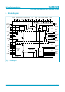
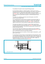
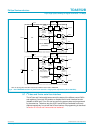
The calibration of the gains is done using the following principle.
From the reference voltage V
ref
a reference signal of 0.156 V (p-p) (
1
⁄
16
V
ref
) is
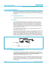
generated internally. During the synchronization part of the video line, the multiplexer,
controlled by the TTL synchronization signal (HSYNCI, coming from HSYNC;
see Figure 1) with a width equal to one of the video synchronization signals (e.g. the
signal coming from a synchronization separator), is switched between the two
amplifiers.
The output of the multiplexer is either the normal video signal or the 0.156 V
reference signal (during HSYNC).
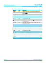
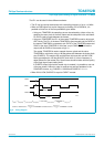
The corresponding ADC outputs are then compared to a preset value loaded in a
register. Depending on the result of the comparison, the gain of the variable gain
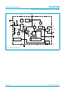
amplifiers is adjusted (coarse gain control; see Figure 2 and 6). The three 7-bit
registers receive data via a serial interface to enable the gain to be programmed.
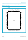
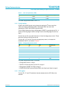
The preset value loaded in the 7-bit register is chosen between approximately
67 codes to ensure the full-scale input range (see Figure 6). A contrast control can be
achieved using these registers. In this case care should be taken to stay within the
allowed code range (32 to 99).
A fine correction using three 5-bit DACs, also controlled via the serial interface, is
used to fine tune the gain of the three channels (fine gain control; see Figure 2 and 7)
and to compensate the channel-to-channel gain mismatch.
With a full-scale ADC input, the resolution of the fine register corresponds to
1
⁄
2
LSB
peak-to-peak variation.
To use these gain controls correctly, it is recommended to fix the coarse gain (to have
a full-scale ADC input signal) to within 4 LSB and then adjust it with the fine gain. The
gain is adjusted during HSYNC. During this time the output signal is not related to the
amplified input signal. The outputs, when the coarse gain system is stable, are
related to the programmed coarse code (see Figure 6).
Fig 6. Coarse gain control.
FCE472
128
160
227
255
0
32
99
127
G
(max)
G
(min)
ADC output
code
N
COARSE
code
coarse
register
value
(67 codes)
0.2
0.6
V
i (p-p)
2
0.156 =
V
ref
16